

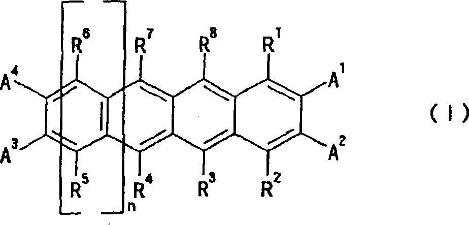
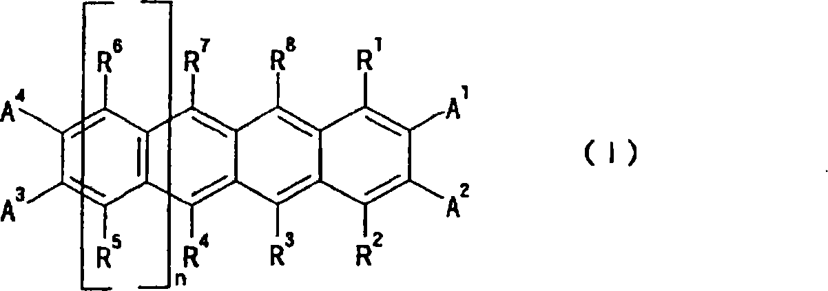
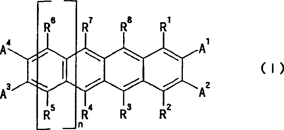
Photoelectric conversion element
A technology for photoelectric conversion elements and photoelectric conversion layers, which can be used in electrical components, photovoltaic power generation, and electric solid-state devices, etc., and can solve problems such as difficulty in obtaining semiconductor layers.
- Summary
- Abstract
- Description
- Claims
- Application Information
AI Technical Summary
Problems solved by technology
Method used
Image

Examples
Embodiment
[0166] Hereinafter, the present invention will be described in more detail through examples, but of course the present invention is not limited to these examples. In addition, each compound obtained by the synthesis example was purified by the sublimation purification method and used in the examples.
Synthetic example 1
[0167] [Synthesis Example 1] Compound 1
[0168] As Compound 1, a commercially available compound (manufactured by Aldrich) having a structure represented by the following [Chemical Formula 7] was used.
[0169] [chemical formula 7]
[0170] (compound 1)
Synthetic example 2
[0171] [Synthesis Example 2] Synthesis of Compound 2
[0172] Compound 2 represented by the following [Chemical Formula 8] was synthesized in the following order.
[0173] [chemical formula 8]
[0174] (compound 2)
[0175] Dissolve zirconocene dichloride in THF, add 2 equivalents of n-butyllithium at -78°C and stir for 1 hour. To this solution, 1 equivalent of the following compound diyne 1 was added and stirred at room temperature to produce the following compound zirconopentadiene 1. Add 2 equivalents of CuCl to it, and add 3 equivalents of N,N-dimethylpropylene urea (DMPU), and 1 equivalent of dimethyl acetylene dicarboxylate (DMAD), and stir at 50°C for 3 hours , the dihydride of compound 2 is generated, and the dihydride is reacted with 1 equivalent of 2,3-dichloro-5,6-dicyanobenzoquinone (DDQ) to obtain compound 2.
[0176] [chemical formula 9]
[0177] (diyne 1)
[0178] (Zirconopentadiene 1)
PUM
| Property | Measurement | Unit |
|---|---|---|
| thickness | aaaaa | aaaaa |
| thickness | aaaaa | aaaaa |
| thickness | aaaaa | aaaaa |
Abstract
Description
Claims
Application Information