Semiconductor device and method for manufacturing the same

A technology of semiconductors and conductors, applied in the field of semiconductor devices and their manufacturing

Inactive Publication Date: 2008-09-03
SONY CORP
View PDF4 Cites 1 Cited by
  • Summary
  • Abstract
  • Description
  • Claims
  • Application Information

AI Technical Summary

Problems solved by technology

The structure of this transistor is slightly different from that of molecular devices previously represented by electrode / molecule / electrode diagrams, in that intermolecular charge movement is not included in the conduction pathway, and mobility is not limited by intermolecular charge movement; thus, fast conduction becomes possible

Method used


Image

  • Semiconductor device and method for manufacturing the same
  • Semiconductor device and method for manufacturing the same
  • Semiconductor device and method for manufacturing the same

Examples


Embodiment 1

[0084] In Embodiment 1, a semiconductor device constituted as an insulated gate type field effect transistor and its manufacturing method are described.

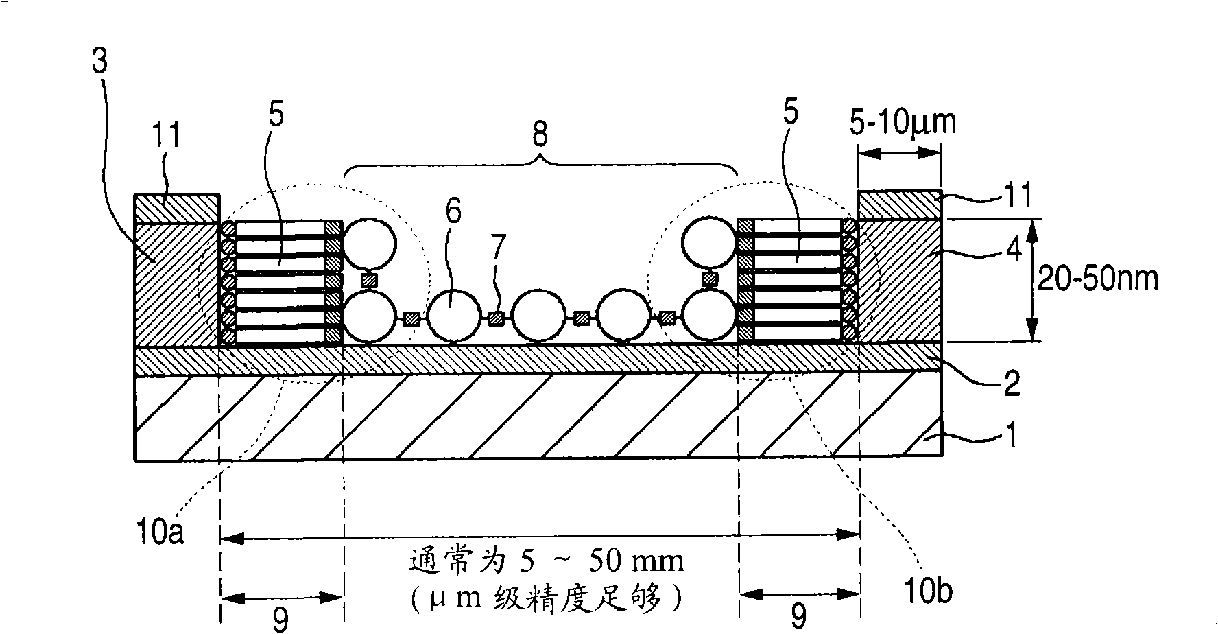
[0085] Figure 1A is a schematic cross-sectional view showing the structure of an insulated gate field effect transistor (FET) 10 based on Embodiment 1. Such as Figure 1A As shown, the transistor 10 is configured as a bottom-gate / bottom-contact FET.

[0086] The substrate 1 also serves as a gate electrode, and is, for example, an n-type silicon substrate doped with impurities and having conductivity. On the surface of the substrate 1 is provided a gate insulating film 2 made of silicon oxide or the like; and a source electrode 3 and a drain electrode 4 each made of gold or the like are provided opposite thereon. An insulating film 11 is provided on each of the source electrode 3 and the drain electrode 4 to cover the top surface thereof.

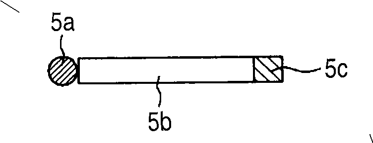
[0087] A monomolecular film composed of organic semiconductor molecules 5 is form...

Embodiment 2

[0121] A semiconductor device configured as an insulated gate type field effect transistor having a top gate type structure and a method of manufacturing the same will be described.

[0122] Figure 4 is a schematic cross-sectional view showing the structure of an insulated gate type field effect transistor (FET) 20 based on Embodiment 2. Since the transistor 20 differs from the insulated gate type field effect transistor (FET) 10 only in that it is a top gate type structure, the insulated gate type field effect transistor 20 is described while emphasizing the different points.

[0123] The substrate 21 is an insulating substrate, and is, for example, a plastic substrate made of polyimide, polycarbonate, polyethylene terephthalate (PET), or the like, a glass substrate, a quartz substrate, mica, or the like. By using a plastic substrate, a semiconductor device having a curved shape (for example, a display having a curved surface shape) can be manufactured.

[0124] A source e...

Embodiment 3

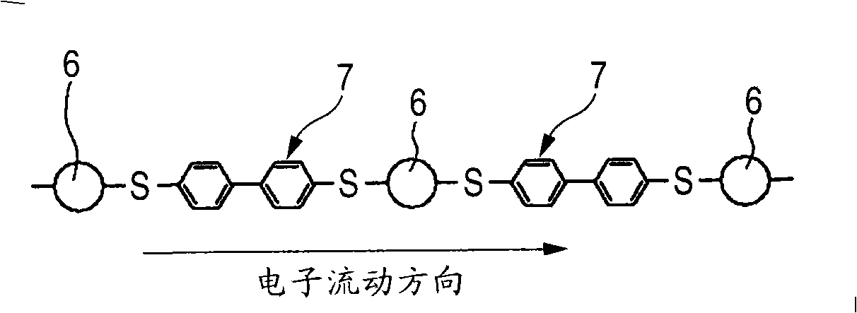
[0135] In Embodiment 3, an insulated gate type field effect transistor is described as an example related to a semiconductor device in which each of the linker molecule and the semiconductor molecule has a highly conductive metal complex moiety in its important portion. In addition, as an example related to its manufacturing method, it is described that the protective film molecule bound to the microparticle is replaced by the first molecule; the first molecule is polymerized with the second molecule to form a precursor molecule bound to the microparticle; the microparticle is set at a designated position and an example of binding adjacent precursor molecules to each other to form a linker molecule.

[0136] Figure 7A is a schematic cross-sectional view showing the structure of an insulated gate type field effect transistor (FET) 30 based on Embodiment 3. Such as Figure 7A As shown, the field effect transistor 30 is constructed similarly to the field effect transistor 10 d...


PUM


Abstract

A semiconductor device is disclosed. The device includes: oppositely disposed plural electrodes; a semiconductor molecule disposed such that one end part thereof binds to a surface of the electrode in each of the opposing electrodes; and a conductor for electrically connecting at least a part of the other end part of the semiconductor molecule disposed in one electrode of the opposing electrodes to at least a part of the other end part of the semiconductor molecule disposed in the other electrode of the opposing electrodes. The conductivity between the opposing electrodes is substantially determined by the conductivity of the semiconductor molecule electrically connected to the conductor between the opposing electrodes in the semiconductor molecules. The channel region of the semiconductor device has high conductivity, unlimited by the charges movement between molecules, and easily and safety prepared.

Description

[0001] Cross References to Related Applications [0002] The present invention contains subject matter related to Japanese Patent Application JP 2007-028679 filed in the Japan Patent Office on Feb. 8, 2007, the entire content of which is hereby incorporated by reference. technical field [0003] The present invention relates to a semiconductor device using semiconductor molecules as a channel material and a method of manufacturing the same. In particular, the present invention relates to a semiconductor device having a channel region with excellent conductivity and which is easy to manufacture and a method for manufacturing the same. Background technique [0004] An organic semiconductor device (for example, an organic transistor) of the related art has a structure represented by an electrode / molecular aggregate / electrode diagram, and an organic semiconductor molecular material in the form of molecular crystals, agglomerated molecular aggregates, etc. is disposed between two...

Claims


Application Information

Patent Timeline
Patent Type & Authority Applications(China)
IPC IPC(8): H01L51/00H01L51/05H01L51/40
CPCB82Y10/00H01L51/0595H01L51/0545H10K10/701H10K10/466
Inventor 保原大介
Owner SONY CORP
Why Eureka
Try Eureka