Supercharge Your Innovation With Domain-Expert AI Agents!

Exhaust device, substrate processing device incorporating same and exhaust method

A substrate processing device, exhaust device technology, applied in electrical components, climate sustainability, greenhouse gas capture, etc., can solve problems such as obstruction of exhaust gas flow, valve malfunction, etc.

Inactive Publication Date: 2008-09-10
PSK INC
View PDF0 Cites 8 Cited by
  • Summary
  • Abstract
  • Description
  • Claims
  • Application Information

AI Technical Summary

Problems solved by technology

That is, the reaction by-products etc. flowing inside the exhaust pipe accumulate on the inner wall of the exhaust pipe, obstructing the flow of exhaust gas, or accumulate on the valve of the opening and closing exhaust pipe, causing the malfunction of the valve

Method used


Image

  • Exhaust device, substrate processing device incorporating same and exhaust method
  • Exhaust device, substrate processing device incorporating same and exhaust method
  • Exhaust device, substrate processing device incorporating same and exhaust method

Examples


Embodiment Construction

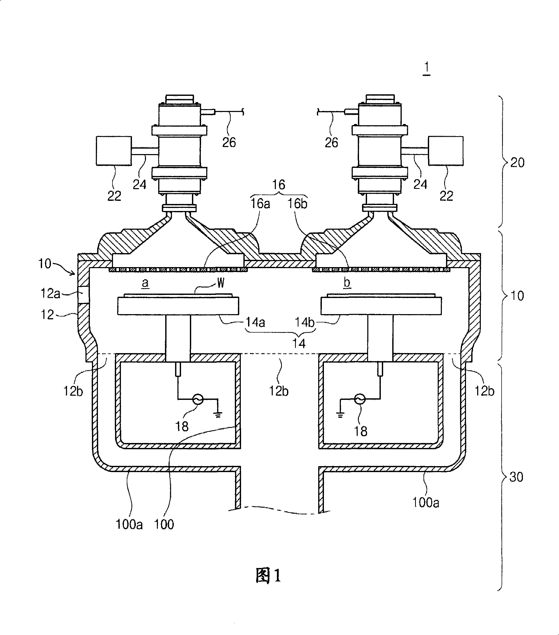
[0047] According to Figure 1- Figure 11 Preferred embodiments of the present invention will be described in detail. Embodiments of the present invention can be changed in various forms, and the scope of the present invention should not be construed as being limited to the embodiments described below. This embodiment is for explaining the present invention in more detail to those having ordinary technical knowledge belonging to the technical field of the present invention. Therefore, the shape of each element shown in the drawings may be somewhat exaggerated for clearer emphasis.

[0048] On the other hand, although an ashing device will be described as an example below, the present invention can be applied to a semiconductor manufacturing device including a cleaning device and a vapor deposition device.

[0049] FIG. 1 is a cross-sectional view schematically showing the structure of a substrate processing apparatus 1 of the present invention.

[0050] As shown in FIG. 1 , ...


PUM


Abstract

The invention provides an air exhaust device, a substrate processing device including the air exhaust device and an air exhaust method. Air in a processing chamber and reaction by-products are exhausted through an air exhaust pipe. An air exhaust port is connected with the air exhaust pipe and collects reaction by-products through the air exhaust port. The air exhaust port includes a collecting canister for containing collected reaction by-products, and a tightening component for connecting the collecting canister with the air exhaust pipe, the collecting canister connects with the air exhaust port that is formed on side wall of the air exhaust pipe. The air exhaust pipe includes a first and a second air exhaust pipes and a connecting pipe, the air exhaust port and a guide surface are formed on the connecting pipe.

Description

technical field [0001] The present invention relates to an exhaust device and method, in particular to an exhaust device and method for collecting reaction by-products in a gas. Background technique [0002] In order to manufacture a semiconductor, a lithography (lithography) process using a photoresist is necessary. The photoresist is composed of an organic polymer or a mixture of a photosensitive agent and a polymer that can be sensitive to light. After exposure and dissolution, a patterned photoresist is formed on the substrate. On the substrate and the substrate During the process of etching the film, the pattern is transferred to the substrate. Such a polymer is called a photoresist, and the process of forming a fine pattern on a substrate using a light source is called a lithography process. [0003] In this kind of semiconductor manufacturing process, photoresist forms various fine circuit patterns such as line or space patterns on the substrate, or is used as a mas...

Claims


Application Information

Patent Timeline
IPC IPC(8): G03F7/42H01L21/00
CPCY02C20/30Y02P70/50G03F7/427H01J37/32844
Inventor 朴正
Owner PSK INC
Features
  • R&D
  • Intellectual Property
  • Life Sciences
  • Materials
  • Tech Scout
  • Unparalleled Data Quality
  • Higher Quality Content
  • 60% Fewer Hallucinations
Learn More