Memory element and manufacturing method thereof

A technology for memory components and manufacturing methods, which is applied in the fields of semiconductor/solid-state device manufacturing, electrical components, semiconductor devices, etc., and can solve problems such as unsatisfactory reliability and uniformity

Inactive Publication Date: 2008-09-24
西格斯教育资本有限责任公司
View PDF0 Cites 22 Cited by
  • Summary
  • Abstract
  • Description
  • Claims
  • Application Information

AI Technical Summary

Problems solved by technology

The heating electrodes of this storage element structure are arranged horizontally. In this way, the size of the heating electrodes is determined by the thickness of the film forming the heating electrodes 202, and is not limited by the yellow photolithography process. However, the phase change of the phase change memory element process The material is deposited by a hole-filling process, and the reliability and uniformity of its contact with the heating electrode 112 are not ideal

Method used


Image

  • Memory element and manufacturing method thereof
  • Memory element and manufacturing method thereof
  • Memory element and manufacturing method thereof

Examples


Embodiment Construction

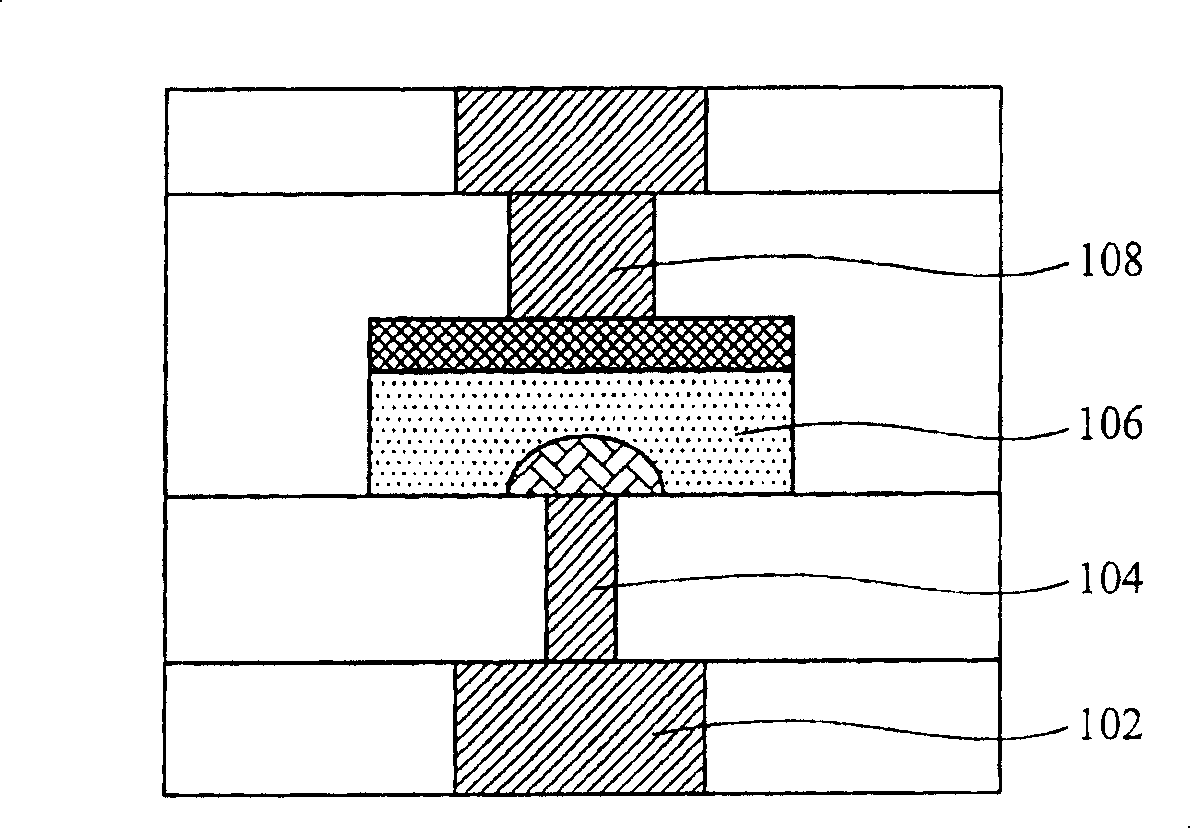
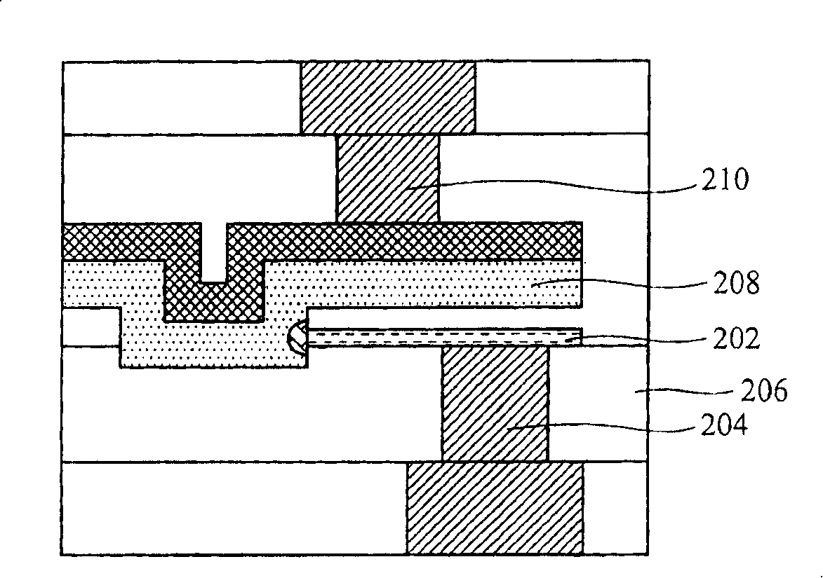
[0057] The following will refer to the present invention in detail with the embodiments, and the examples are accompanied by drawings. In the drawings or descriptions, the same reference numerals are used for similar or identical parts. In the drawings, the shape or thickness of the embodiments may be exaggerated for simplification or convenient labeling. Parts of each element in the drawings will be described separately. It is worth noting that elements not shown or described in the drawings can have various forms known to those skilled in the art. In addition, the specific embodiment is only A specific method used in the present invention is disclosed, which is not intended to limit the present invention.

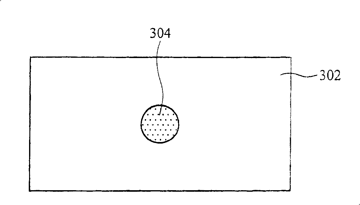
[0058] Figure 3A ~ Figure 10B A method for manufacturing a phase-change memory element according to an embodiment of the present invention is disclosed, wherein Figure 3A for Figure 3B The top view of the , first, refer to the Figure 3A and Figure 3B , providin...


PUM


Abstract

The invention relates to a memory element. A cylindrical structure comprises a first electrode layer, a dielectric layer on the first electrode layer and a second electrode layer on the dielectric layer. A phase change layer coats around the cylindrical structure. A bottom electrode is electrically connected with the first electrode layer of the cylindrical structure. A top electrode is electrically connected with the second electrode layer of the cylindrical structure.

Description

technical field [0001] The invention relates to a semiconductor element and a manufacturing method thereof, in particular to a memory element and a manufacturing method thereof. Background technique [0002] Phase-change memory has competitive characteristics such as speed, power, capacity, reliability, process integration and cost, and is suitable for high-density stand-alone or embedded memory applications. Due to the unique advantages of phase change memory technology, it is also considered very likely to replace the current commercially competitive static memory SRAM and dynamic random access memory DRAM volatile memory and flash memory Flash non-volatile memory technology, It is expected to become a new era semiconductor memory with great potential in the future. [0003] The phase-change memory element utilizes the difference in the resistance value of the phase-change memory material in the crystalline state and the amorphous state to perform writing, reading or eras...

Claims


Application Information

Patent Timeline
Patent Type & Authority Applications(China)
IPC IPC(8): H01L21/82H01L21/28H01L27/24H01L45/00
Inventor 俞笃豪
Owner 西格斯教育资本有限责任公司
Why Eureka
Try Eureka