Electric voltage peak absorption circuit of DC converter power switch pipe

A technology of power switching tube and DC converter, which is applied in the field of switching power supply, and can solve the problems of restricting the overall efficiency of the converter and improving it.

Inactive Publication Date: 2008-09-24
YIBO POWER SUPPLY CO LTD HANGZHOU
View PDF0 Cites 24 Cited by
  • Summary
  • Abstract
  • Description
  • Claims
  • Application Information

AI Technical Summary

Problems solved by technology

After Rs is determined, its loss is: VCs 2 / Rs, this loss restricts the improvement of the overall efficiency of the converter to a considerable extent

Method used


Image

  • Electric voltage peak absorption circuit of DC converter power switch pipe
  • Electric voltage peak absorption circuit of DC converter power switch pipe
  • Electric voltage peak absorption circuit of DC converter power switch pipe

Examples


Embodiment 1

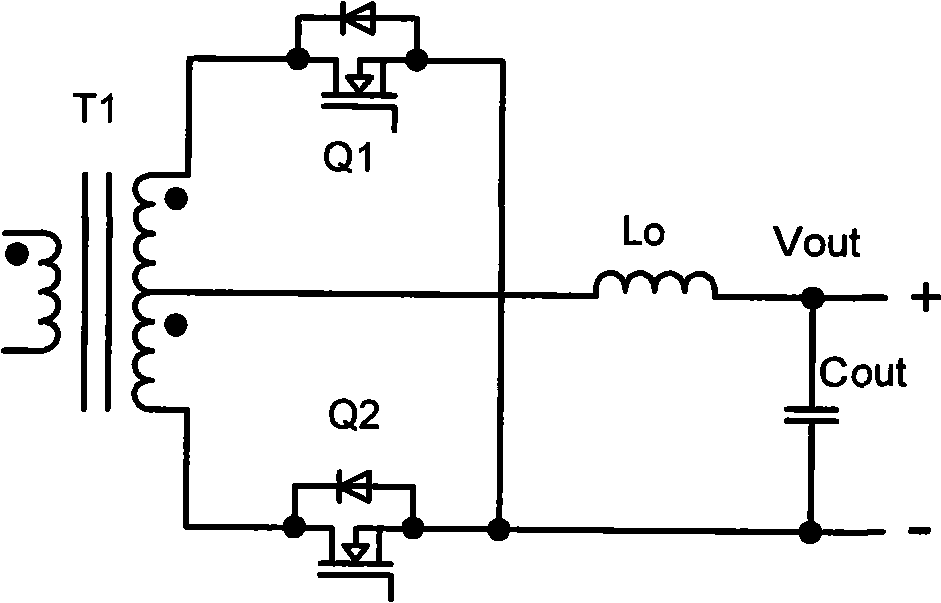
[0029] Figure 7 It is a schematic diagram of the application of the present invention in a bridge full-wave rectifier circuit. Since the snubber circuit in this embodiment is used for the power switch tube on the secondary side of the converter, the power switch tube is a rectifier power tube. The converter includes a main transformer T1, a first rectifying power tube Q1 and a second rectifying power tube Q2, and the absorbing circuit includes a first clamping diode Ds1 and a second clamping diode corresponding to the rectifying power tube. Diode Ds2, a snubber capacitor Cs, a snubber switch Qs, a protection diode Dp, an anti-current backfeed diode Df, a freewheeling diode D, a filter inductor L and a drive resistor R, the clamp The anodes of the bit diodes Ds1 and Ds2 are respectively connected to the drains of the rectifier power transistors Q1 and Q2, the cathode is connected to one end of the absorbing capacitor Cs and the collector of the absorbing switch Qs, and the em...

Embodiment 2

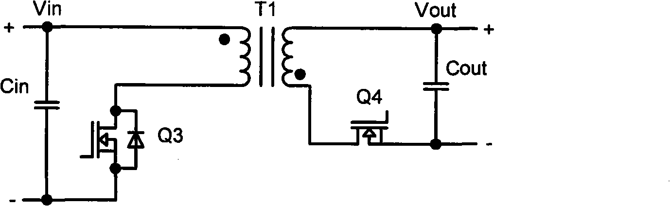
[0044] Figure 10 It is a schematic diagram of the application of the present invention on the primary side of the flyback circuit. The converter includes a transformer T1 and a primary power switch tube Q3, and the snubber circuit includes a clamping diode Ds, a snubber capacitor Cs, a snubber switch Qs, an anti-current backfill diode Df, a freewheeling diode D, Filter inductor L, drive resistor R, protection diode Dp. The anode of the clamping diode Ds is connected to the absorbed clamping end bridge arm of the primary power transistor Q3 of the flyback circuit, that is, the drain of Q3, and the cathode is connected to one end of the absorbing capacitor Cs. The collector of the absorbing switch tube Qs is connected, the emitter of the absorbing switch tube Qs is connected with the anode of the anti-current backfeed diode Df, the cathode of the anti-current backfeed diode Df is connected with the cathode of the freewheeling diode D and the filter One end of the inductor L i...

Embodiment 3

[0048] Figure 13 It is a schematic diagram of the application of the present invention on the secondary side of the flyback circuit. The absorbing circuit includes: transformer T1, secondary side rectifying power tube Q4 clamping diode Ds, absorbing capacitor Cs, absorbing switch tube Qs, anti-current backfilling diode Df, freewheeling diode D, filter inductor L, drive resistor R, protection diode Dp. The anode of the clamping diode Ds is connected to the absorbed clamping end bridge arm of the flyback circuit secondary side power tube rectifier tube Q5, that is, the drain of Q5, and the cathode is connected to one end of the absorbing capacitor Cs. Also connected to the collector of the snubber switch Qs, the emitter of the snubber switch Qs is connected to the anode of the anti-current backfeed diode Df, the cathode of the anti-current backfeed diode Df is connected to the cathode of the freewheeling diode D and One end of the filter inductor L is connected, the other end...


PUM


Abstract

An absorption circuit for a voltage spike of a switching tube of a DC converter power includes: a transformer T1, a first commuting power tube Q1, a second commuting power tube Q2, a first clamp diode Ds1, a first clamp diode Ds2, an absorption capacitance Cs, an absorption switching tube Qs, a current reverse irrigation preventing diode Df, a fly-wheel diode D, a filter inductance L, a drive resistance R and a protection diode Dp. The invention is mainly characterized in that the absorption switching tube Qs is driven by a bridge arm square wave through driving the drive resistance R; the output of the absorption circuit is connected with the output of a power. The invention can effectively absorb the voltage spike of the power switching tube, reduce the voltage stress, improve the efficiency of the converter, and has characteristics of comparatively simple structure and reliable performance.

Description

technical field [0001] The invention relates to a switching power supply, in particular to a circuit for absorbing and clamping the voltage peak of a power switching tube of a switching type DC converter. Background technique [0002] The power switching tube in the switch-type DC converter usually works in a hard switching state. There are parasitic oscillations on the primary side and the secondary side of the transformer during the commutation, and the power switching tube usually bears a high peak voltage. [0003] figure 1 It is the schematic diagram of the DC converter with full-wave rectification on the secondary side. The rectifier power tubes Q1 and Q2 in the full-wave rectification circuit of the transformer continue to flow during the period when the primary switch tubes are simultaneously cut off. During freewheeling, the sum of the currents flowing through Q1 and Q2 is equal to the current flowing through the output inductor Lo. When reverse excitation reappe...

Claims


Application Information

Patent Timeline
Patent Type & Authority Applications(China)
IPC IPC(8): H02M1/32H02H9/04
Inventor 唐钊徐迎春周远平
Owner YIBO POWER SUPPLY CO LTD HANGZHOU
Why Eureka
Try Eureka