Analog switch chip design method and chip device

An analog switch chip and design method technology, applied in electronic switches, electrical components, pulse technology, etc., can solve the problems of affecting the operating bandwidth, performance mutual restraint, limiting the turn-off isolation performance of analog switches, etc., to improve the charge injection performance. , the effect of eliminating the offset effect

Inactive Publication Date: 2008-09-24
方泰开曼公司
View PDF0 Cites 9 Cited by
  • Summary
  • Abstract
  • Description
  • Claims
  • Application Information

AI Technical Summary

Problems solved by technology

[0003] The performance indicators of the analog switch chip mainly include on-resistance, bandwidth, off-isolation, and charge injection. Currently, under the standard CMOS process, the technology of eliminating the substrate bias effect of the analog switch basically adopts certain circuit architectures to realize the PMOS tube lining. The selection of the bottom voltage can eliminate the lining offset effect and improve the on-resistance performance. However, due to the mutual constraints of the four properties, there are few methods that can simultaneously improve the bandw

Method used


Image

  • Analog switch chip design method and chip device
  • Analog switch chip design method and chip device
  • Analog switch chip design method and chip device

Examples


Embodiment Construction

[0018] The present invention will be described in detail below in conjunction with a specific embodiment circuit.

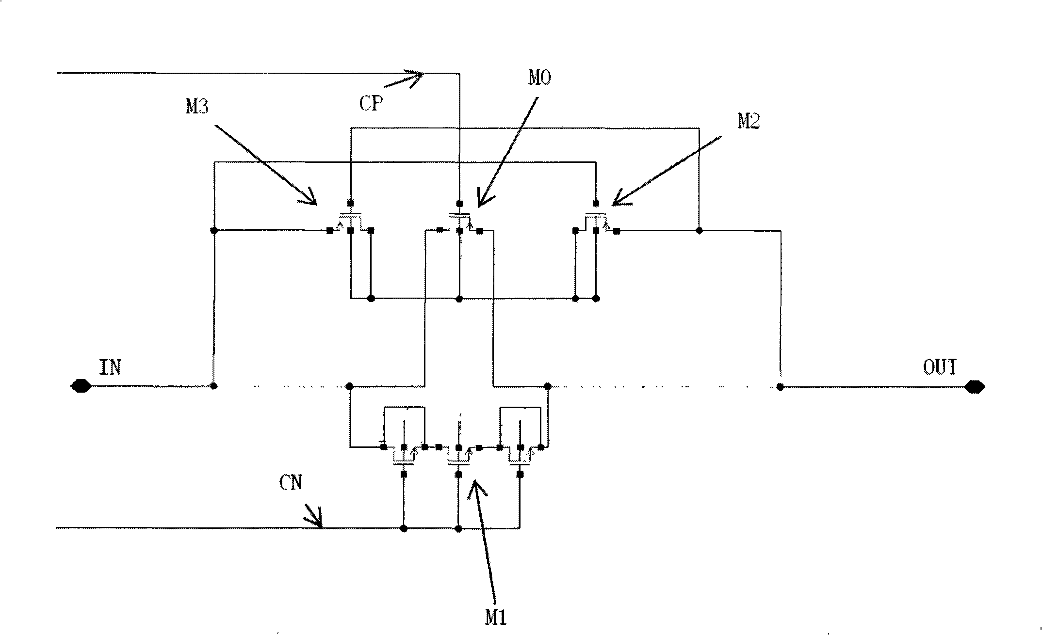
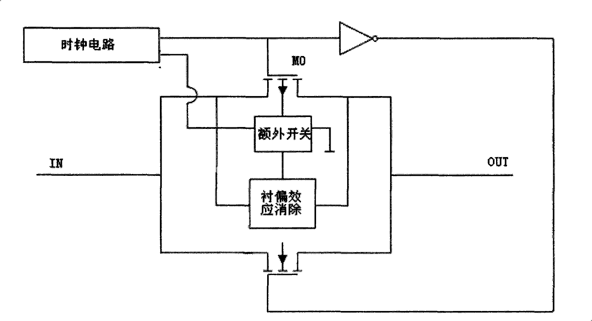
[0019] As attached figure 2 Schematic diagram of the circuit, the key point of the present invention is to use an additional switch controlled by the clock circuit to make the offset elimination circuit work under certain conditions, so that the substrate of the main switch MOS is connected to the relatively high potential end of the input and output terminals ; When the main switch is turned off, the substrate is directly connected to the power source to avoid the adverse effects of the offset elimination circuit on the main switch.

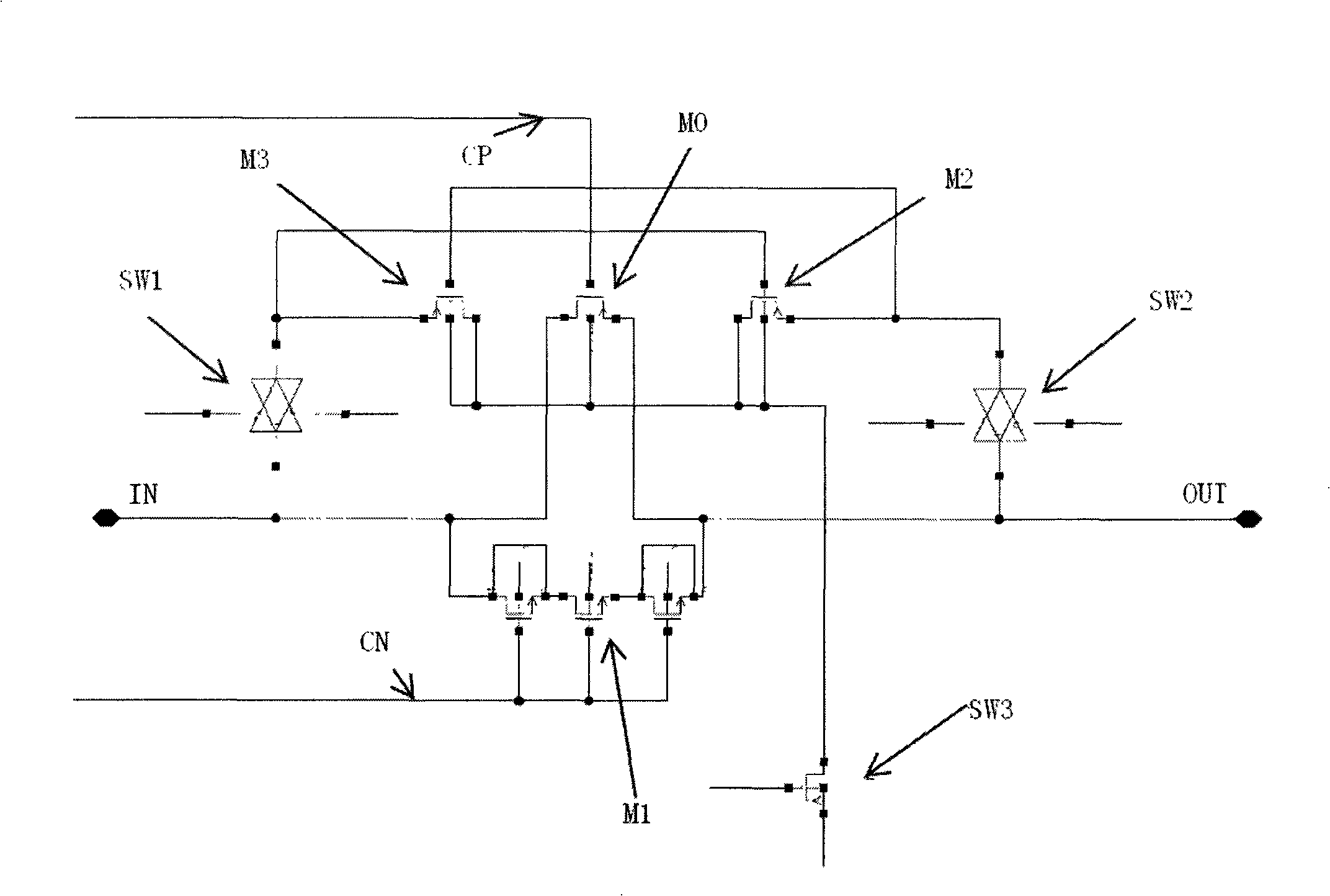
[0020] We take PMOS as an example, as attached image 3 It is a detailed circuit diagram of a specific embodiment of the analog switch chip of the present invention, and attached figure 1 Compared with the standard CMOS process analog switch circuit with offset elimination circuit shown, it can be clearly seen that M0 and M1 are the ...


PUM


Abstract

The invention provides a design method of an analog switch chip which controls the time sequence by a clock circuit and controls the work of the substrate bias canceling circuit of a main switch MOS in a standard CMOS technique analog switch circuit by an additional switch module. The invention also provides a chip device which comprises a standard CMOS technique analog switch circuit, a substrate bias canceling circuit, an additional switch module and a clock circuit. The substrate bias canceling circuit is connected with the substrate of the main switch MOS; a secondary switch provided by the additional switch module is respectively connected with the substrate bias canceling circuit and a power supply voltage; the clock circuit provides a chip device control time sequence. The analog switch chip of the invention improves the bandwidth of the analog switch as well as the turn-off isolation and charge injection properties of the analog switch, which simultaneously ensures the substrate bias effect to be cancelled and improves the conducting impendence property.

Description

Technical field [0001] The invention relates to the field of chip design, in particular to a method and device for designing an analog switch chip. Background technique [0002] In the standard CMOS process, the ideal working state of MOS always assumes that the source region and the substrate are grounded together, that is, Vbs is equal to 0, but in actual working states, the substrate and the source are often disconnected, and Vbs is not equal to 0. It can be known from the basic PN junction theory that the depletion layer of the PN junction in the reverse bias will expand. In addition, the substrate bias Vbs will have a series of effects on the characteristics of the MOSFET. In order to ensure the direction bias of the PN junction between the source-substrate and the drain-substrate, for n-channel devices, the substrate is usually connected to a negative bias. For p-channel devices, the substrate is positively biased, or the MOS substrate and the source region are directly sho...

Claims


Application Information

Patent Timeline
IPC IPC(8): H03K17/687H03K17/14
Inventor 刘晓云林秀龙何金国
Owner 方泰开曼公司
Why Eureka
Try Eureka