Semiconductor device

A semiconductor and device technology, applied in the field of semiconductor devices, can solve the problems of operational amplifier oscillation and larger chip size, etc.

Inactive Publication Date: 2008-10-01
PANASONIC CORP
View PDF2 Cites 4 Cited by
  • Summary
  • Abstract
  • Description
  • Claims
  • Application Information

AI Technical Summary

Problems solved by technology

Therefore, for example, the voltage between the terminals of the phase compensation capacitor 86 of the operational amplifier in FIG. High chance of op amp oscillation
[0016] In addition, in order to avoid the possibility of oscillation even under the use condition that (VOUT-V1) becomes near 0V, it is necessary to make the phase compensation capacitor 86 very large, and there is a problem that the chip size becomes large.

Method used


Image

  • Semiconductor device
  • Semiconductor device
  • Semiconductor device

Examples


Embodiment approach 1

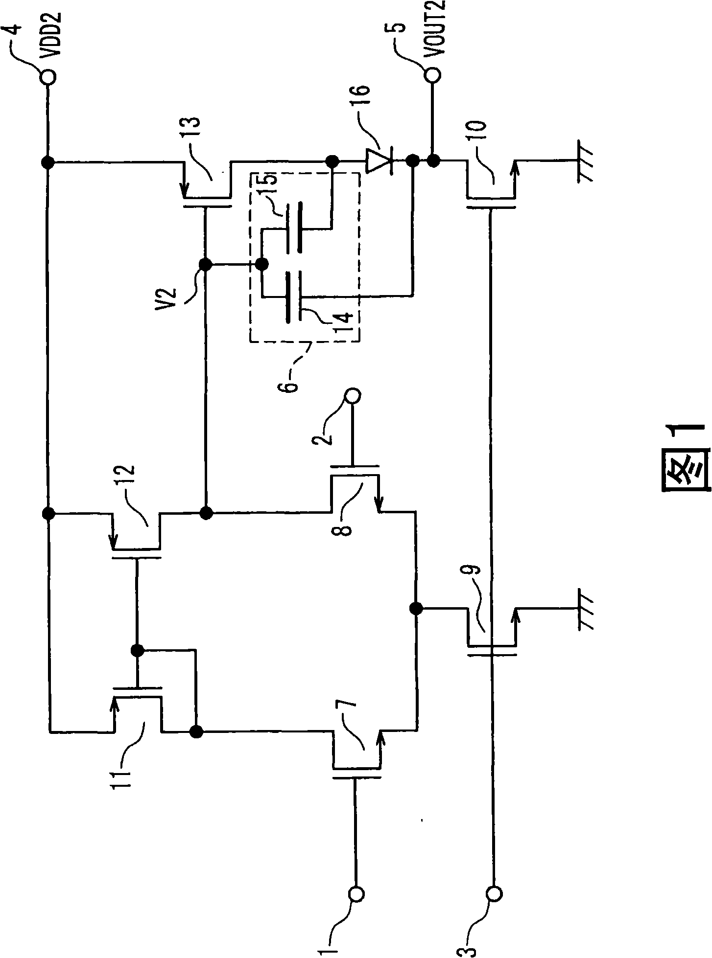
[0037]FIG. 1 shows a semiconductor device in Embodiment Mode 1 of the present invention. The N-channel MOS transistor 7 and the N-channel MOS transistor 8 constitute a differential input stage portion, and signals from the inverting input terminal 1 and the non-inverting input terminal 2 are input to respective gates. The source of the MOS transistor 7 and the source of the MOS transistor 8 are connected to each other, and a constant current is introduced from the drain of the N-channel MOS transistor 9 . The drain current of the MOS transistor 9 is set by the voltage of the bias voltage input terminal 3 .

[0038] The sources of the P-channel MOS transistors 11 and 12 are commonly connected to the power supply terminal 4 (high side power supply VDD2 ). The drain of the MOS transistor 7 is connected to the gates of the MOS transistors 11 and 12 and the drain of the MOS transistor 11 , and the drain of the MOS transistor 8 is connected to the drain of the MOS transistor 12 . ...

Embodiment approach 2

[0056] A semiconductor device according to Embodiment 2 of the present invention will be described with reference to FIG. 6 . This semiconductor device is an operational amplifier composed of bipolar transistors, MOS capacitors, diodes, and resistors. It is an example of a circuit that provides negative feedback from the output terminal to the inverting input terminal to buffer the input voltage (increase the current capability). .

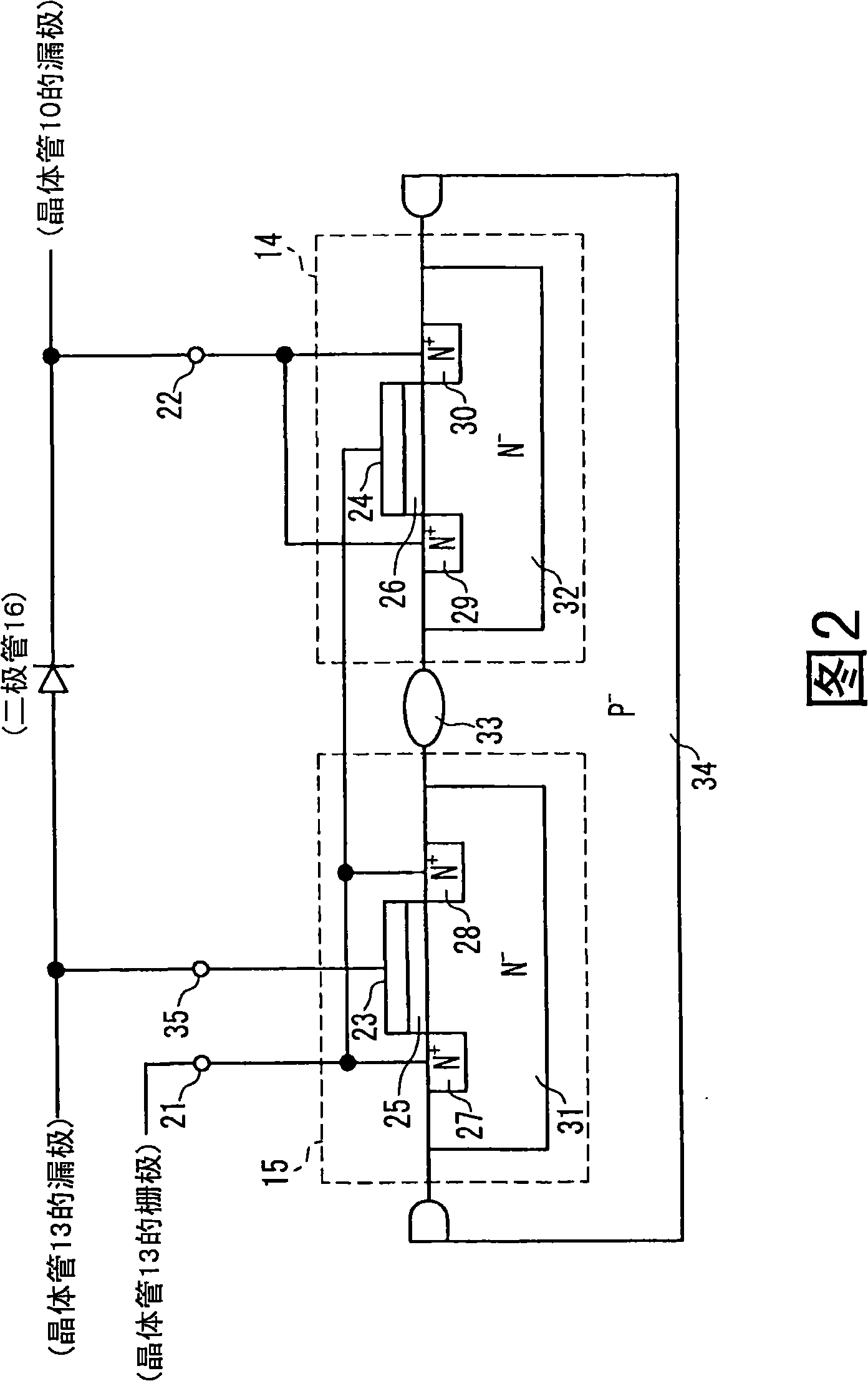
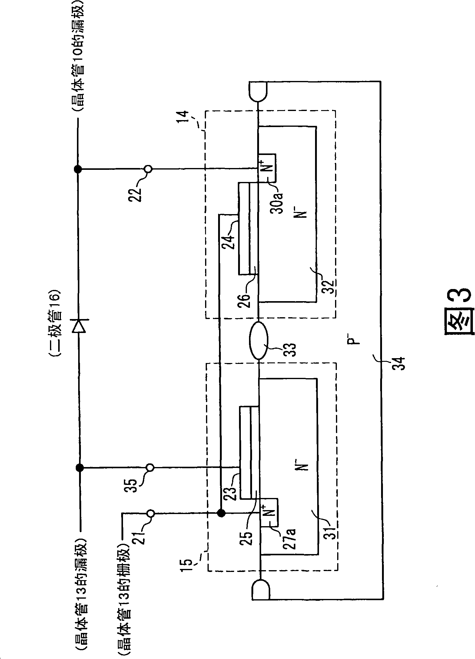
[0057] In Figure 6, 51-60 are PNP transistors, 61-64 are NPN transistors, 65 are diodes, 66-70 are resistors, 71 and 72 are MOS capacitors, 73 are constant current sources, 74 are high-side power supplies, and 75 are output Terminal 76 is a non-reversing input terminal, and 77 is a variable power supply. As the MOS capacitors 71 and 72, a structure having a gate oxide film between the gate electrode and the P well layer can also be considered. Here, as shown in FIG. 2 or FIG. In the case of a capacitor with a structure having a gate oxide film b...


PUM


Abstract

A semiconductor device includes a phase compensation circuit 6 using a MOS capacitor with a structure in which an insulating film is disposed between a gate electrode formed on a semiconductor substrate and a diffusion layer. The phase compensation circuit includes first and second MOS capacitors 14, 15 . A gate electrode terminal of the first MOS capacitor is connected equivalently to a diffusion layer terminal of the second MOS capacitor that is a terminal opposite to the gate electrode terminal. A potential difference generating element 16 that generates a potential difference by allowing a current to flow therethrough is connected between a diffusion layer terminal of the first MOS capacitor and a gate electrode terminal of the second MOS capacitor. When the MOS capacitors having the voltage dependence are used, e.g., as a phase compensation circuit element of an operational amplifier, the MOS capacitance is not reduced, no matter the range of the input or output voltage of the operational amplifier, so that the phase margin will not reduced.

Description

technical field [0001] The present invention relates to a semiconductor device using a voltage-dependent MOS capacitor as a phase compensation circuit element such as an operational amplifier. Background technique [0002] In a conventional semiconductor device, when a MOS capacitor is used as a capacitor for phase compensation such as an operational amplifier, two MOS capacitors are used by connecting terminals of opposite polarities to each other in parallel. The MOS capacitor refers to a capacitor formed on a semiconductor substrate and having an insulating film (gate oxide film) structure between a gate electrode and a diffusion layer. Hereinafter, a "CMOS operational amplifier" disclosed in Japanese Patent Application Laid-Open No. 10-270957, which is a conventional semiconductor device, will be described with reference to FIG. 7 . [0003] In FIG. 7 , N-channel MOS transistor 87 and N-channel MOS transistor 88 constitute a differential input stage portion, and signals...

Claims


Application Information

Patent Timeline
IPC IPC(8): H03F3/45H03F1/34H01L27/06H01L23/522
CPCH03F1/14H03F3/45183H03F2200/153H03F2203/45466H03F2203/45512H03F2203/45641H03F2203/45654H03F2203/45674
Inventor 片冈伸一郎矢野刚广
Owner PANASONIC CORP
Why Eureka
Try Eureka