Multiple independent serial link memory

A technology of memory and flash memory, applied in the direction of static memory, read-only memory, digital memory information, etc.

Inactive Publication Date: 2008-10-01
CONVERSANT INTPROP MANAGEMENT INC
View PDF2 Cites 26 Cited by
  • Summary
  • Abstract
  • Description
  • Claims
  • Application Information

AI Technical Summary

Problems solved by technology

As memory devices operate at increased speeds, crosstalk becomes an increasing issue

Method used


Image

  • Multiple independent serial link memory
  • Multiple independent serial link memory
  • Multiple independent serial link memory

Examples


Embodiment Construction

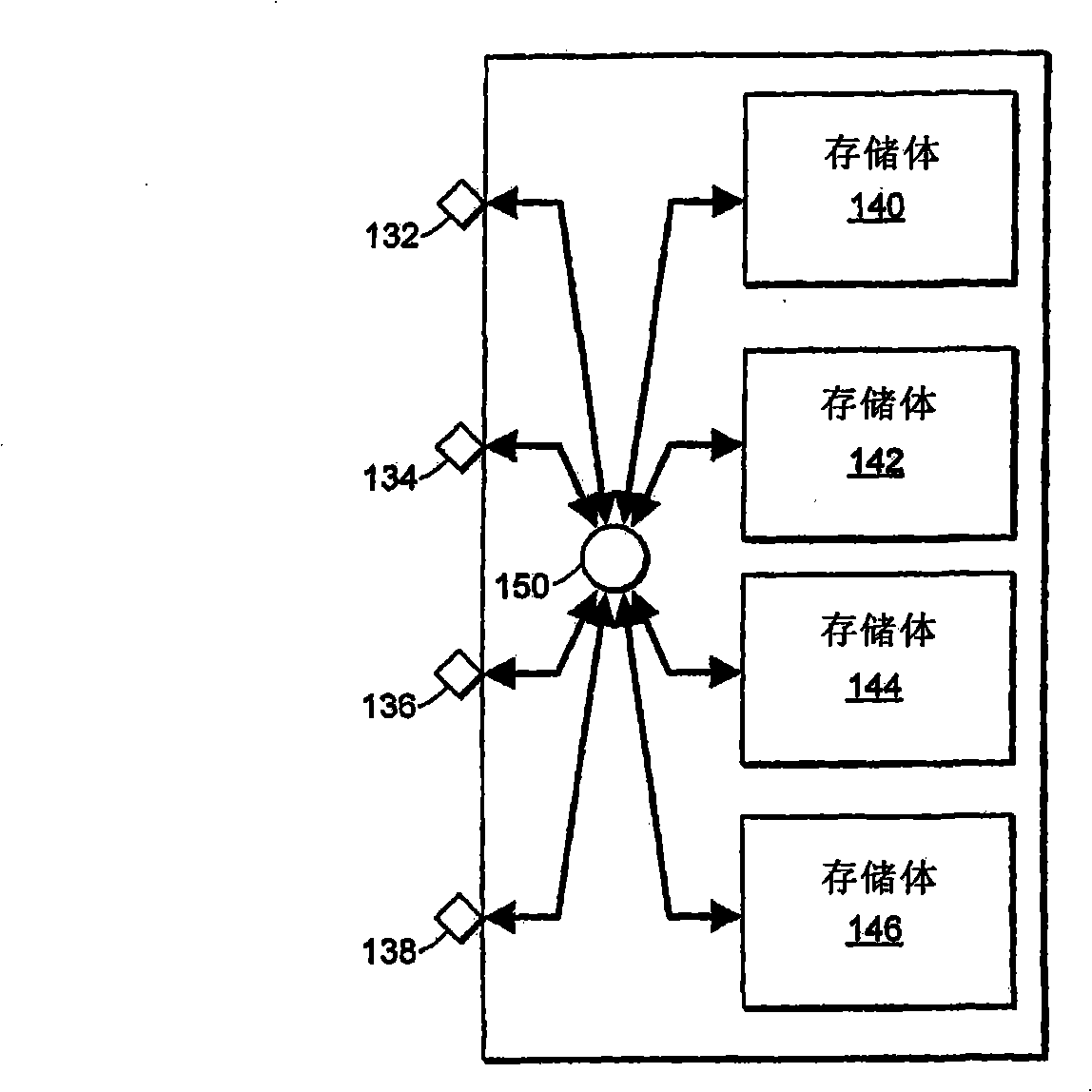
[0026] The invention discloses a serial data interface of a semiconductor memory with at least two memory banks. The serial data interface can include one or more serial data links communicating with the central control logic, wherein each serial data link can receive commands and data serially, and can provide output data serially. Each serial data link can access any bank in the memory for programming and reading data. At least one advantage of the serial interface is the low pin count devices with standard output pins at different densities, thus allowing future compatible upgrades to higher densities without board redesign.

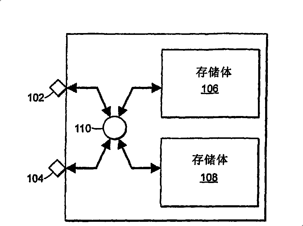
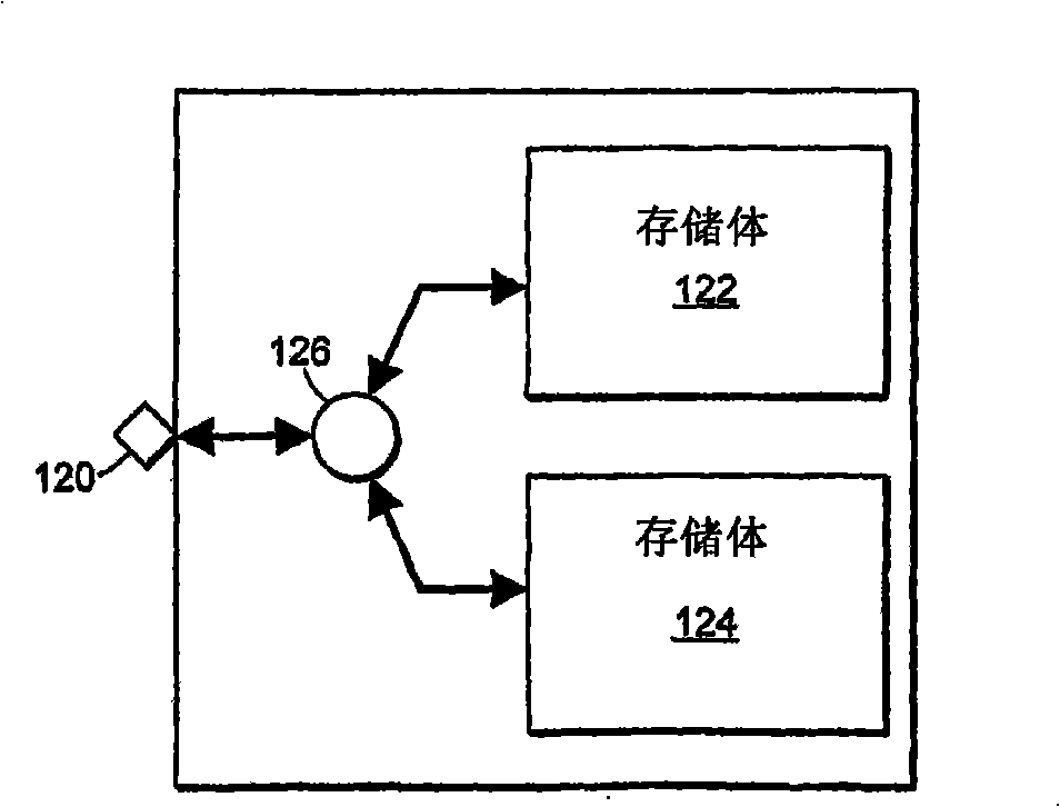
[0027] Figure 1A and 1B A high-level diagram illustrating an exemplary memory device supporting concurrent operations in accordance with aspects of the present invention. Figure 1A A memory device is shown having multiple serial data link interfaces 102 and 104 and multiple memory banks 106 and 108 . The arrangement shown here is referred to as a ...


PUM


Abstract

An apparatus, system, and method for controlling data transfer between a serial data link interface and memory banks in a semiconductor memory is disclosed. In one example, a flash memory device with multiple serial data links and multiple memory banks, where the links are independent of the banks, is disclosed. The flash memory devices may be cascaded in a daisy-chain configuration using echo signal lines to serially communicate between memory devices. In addition, a virtual multiple link configuration is described wherein a single link is used to emulate multiple links.

Description

technical field [0001] The present invention relates to semiconductor memory devices, and more particularly, the present invention relates to a memory structure for increasing the speed and / or capacity of semiconductor flash memory devices. Background technique [0002] Mobile electronic devices such as digital cameras, portable digital assistants, portable audio / video players, and mobile terminals have long required mass memory, preferably non-volatile memory with ever increasing capacity and speed capabilities. For example, currently used audio players may have between 256Mbytes to 40Gbytes of memory for storing audio / video data. Non-volatile memory such as flash memory and hard drives are preferred due to their ability to retain data in the absence of power, thus extending battery life. [0003] Currently, hard disk drives have a high density that can store 20-40G bytes of data, but are relatively bulky. However, flash memory, also known as a solid-state drive, has gain...

Claims


Application Information

Patent Timeline
Patent Type & Authority Applications(China)
IPC IPC(8): G11C11/4193G11C11/4197G11C16/06
CPCG11C7/1021G11C7/1051G11C7/1078G11C16/06G11C2207/107
Inventor 金镇祺潘弘柏
Owner CONVERSANT INTPROP MANAGEMENT INC
Why Eureka
Try Eureka