
Sealing apparatus, sealing method and encapsulation method of integrated circuit chip

A technology of integrated circuits and sealing devices, which is applied in the direction of circuits, electrical components, and electrical solid devices, to achieve the effects of low production costs, broad market prospects, and low investment

Active Publication Date: 2008-10-15
HIERSTAR SUZHOU
View PDF0 Cites 13 Cited by
  • Summary
  • Abstract
  • Description
  • Claims
  • Application Information

AI Technical Summary

Problems solved by technology

[0005] In order to solve the problems of colloidal height, colloidal shape, and cost that occur in packaging ultra-thin chips in the prior art, the purpose of the present invention is to propose a method for encapsulating integrated circuit chips, devices and packaging methods for integrated circuit chips, so as to control the colloid. The height difference between the highest surface height and the highest point of the state line arc is less than 50um, and the regular colloidal shape realizes low-cost integrated circuit chip packaging

Method used


Image

  • Sealing apparatus, sealing method and encapsulation method of integrated circuit chip
  • Sealing apparatus, sealing method and encapsulation method of integrated circuit chip
  • Sealing apparatus, sealing method and encapsulation method of integrated circuit chip

Examples


Embodiment Construction

[0056] The technical solutions of the embodiments of the present invention will be described in further detail below with reference to the drawings and embodiments.

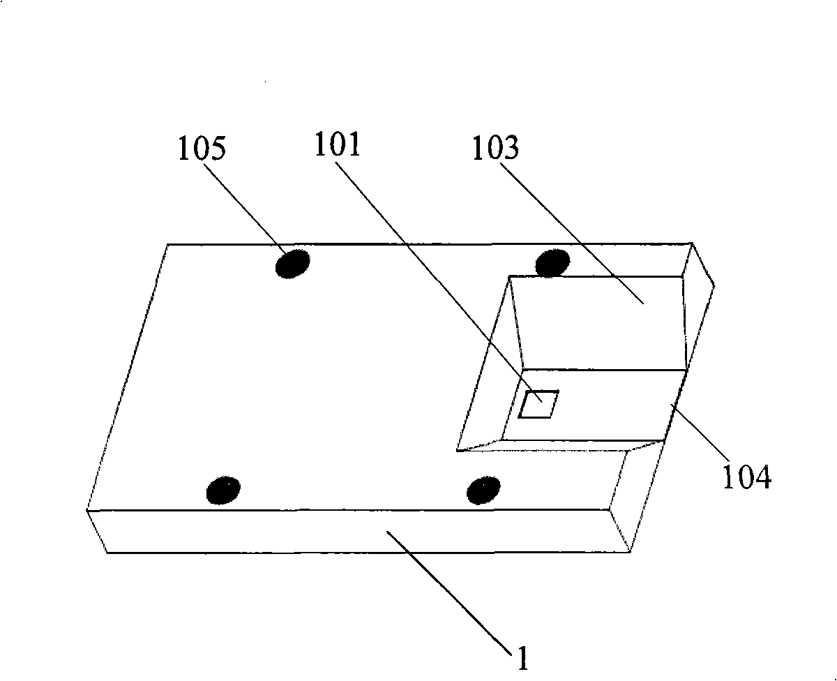
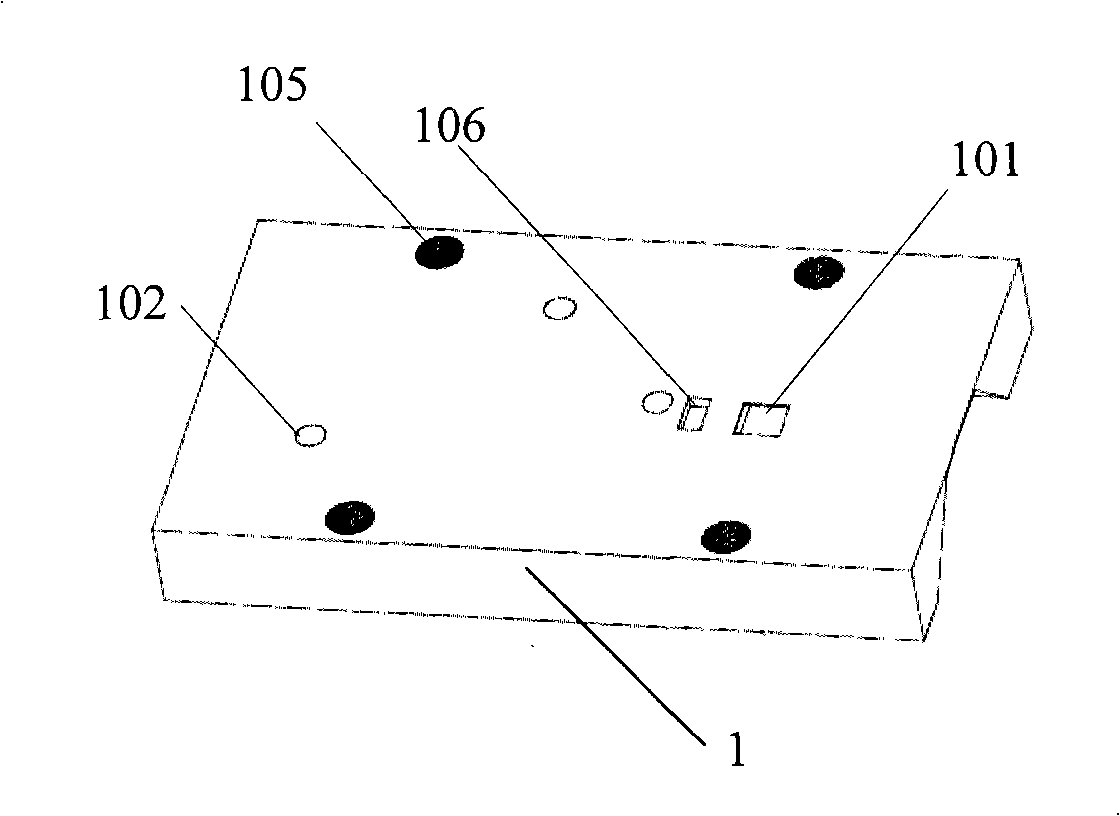
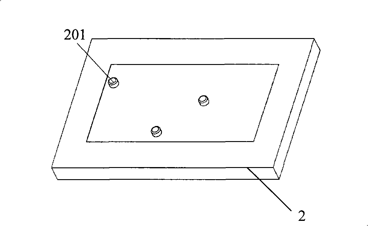
[0057] The present invention provides a kind of sealing glue device of integrated circuit chip, to guarantee the shape and the thickness of the encapsulation epoxy resin on the surface of IC chip, the glue sealing device of the present invention comprises figure 1 and 2 the top plate 1 shown; and image 3 The bottom plate 2 shown is used to support a circuit board with integrated circuit chips. The top plate 1 is fastened with the bottom plate 2, so that the circuit board and the bottom surface of the top plate are closely attached, and the top plate has at least one window corresponding to the position of the integrated circuit chip on the circuit board, so that the chip is completely exposed Come out to pour the sealant.

[0058] Such as figure 1 As shown, it is a schematic diagram of the top surface of the...


PUM


Abstract

The invention discloses a molding device of an integrated circuit chip, comprising a bottom plate used for bearing a circuit board provided with the integrated circuit chip, and a top board used for being buckled with the bottom board and leading the circuit board and the bottom surface of the top board to joint closely; wherein, the top board is provided with at least one opening window corresponding to the position of the integrated circuit chip on the circuit board, thus leading the chip to be exposed completely so as to pour and mold conveniently; the invention also provides a molding method and a packaging method of the integrated circuit chip. The molding device of the integrated circuit chip has low investment and production cost, is economic and practical and realizes the packaging of the ultrathin chip; the thickness of colloid can be controlled under 50um and the molding shape of the chip is regular.

Description

technical field [0001] The invention relates to the field of integrated circuit chip packaging, in particular to an ultra-thin integrated circuit chip sealing device, sealing method and packaging method. Background technique [0002] The development trend of miniaturization, portable, and ultra-thin electronic systems has driven a sharp increase in the demand for miniaturization and flat chip packaging technology. At present, there are two main forms of bare chip technology: one is flip chip technology (Flip chip, FC chips are installed face-down on the PCB), and the other is COB (Chip On Board, COB chips are mounted directly on the PCB face-up) technology. [0003] Flip chip technology: Flip chip is also called flip chip, also known as "flip chip". Compared with COB, flip-chip (FC) has a chip structure and I / O terminals (solder balls) placed under the crystal in this packaging form. Since the I / O terminals are distributed on the entire chip surface, the packaging density a...

Claims


Application Information

Patent Timeline
IPC IPC(8): H01L21/56
CPCH01L2224/48091
Inventor 谢学理张徵郭吉祥谢涛令赵卫民王科宇
Owner HIERSTAR SUZHOU
Learn More