Supercharge Your Innovation With Domain-Expert AI Agents!

Leadframe and flip chip type semiconductor package using leadframe as chip supporter

A lead frame and semiconductor technology, applied in the direction of semiconductor devices, semiconductor/solid-state device components, electrical components, etc., can solve the problems affecting the reliability of semiconductor packages 2, delamination of ground plane 221 and packaging colloid 23, large thermal stress, etc. question

Inactive Publication Date: 2008-10-15
SILICONWARE PRECISION IND CO LTD
View PDF4 Cites 2 Cited by
  • Summary
  • Abstract
  • Description
  • Claims
  • Application Information

AI Technical Summary

Problems solved by technology

Although the semiconductor package 2 has a large ground plane 221 to improve electrical properties and heat dissipation efficiency, the ground plane 221 only has its side 221a and part of the top surface 221b combined with the encapsulant 23, so that the ground plane 221 and the package The bonding between the colloids 23 is insufficient, and it is easy to make the ground plane 221 and the encapsulation colloid 23 between the ground plane 221 and the encapsulation colloid 23 due to the difference in coefficient of thermal expansion (CTE Mismatch) between the materials of the ground plane 221 and the encapsulation colloid 23 in the subsequent thermal cycle (Thermal Cycling). Delamination of the joint surface occurs, such as Figure 2C As shown in D in the figure; once delamination occurs, it will lead to the intrusion of water vapor and the Popcorn Effect, which will affect the reliability of the semiconductor package 2
In addition, due to the large area of ​​the ground plane 221 , greater thermal stress will be generated during the thermal cycle, which will more easily lead to the delamination of the ground plane 221 and the encapsulant 23

Method used


Image

  • Leadframe and flip chip type semiconductor package using leadframe as chip supporter
  • Leadframe and flip chip type semiconductor package using leadframe as chip supporter
  • Leadframe and flip chip type semiconductor package using leadframe as chip supporter

Examples


no. 1 example

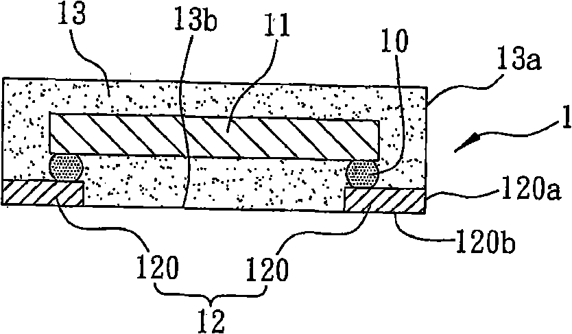
[0067] refer to Figure 3A and Figure 3B As shown, it is the top view and the edge view of the flip-chip semiconductor package according to the first embodiment of the present invention. Figure 3A A sectional view taken along line 3B-3B is shown.

[0068] As shown in the figure, the semiconductor package 3 is composed of a chip 31, a lead frame 32 for carrying the chip 31, a plurality of solder bumps 30a and ground bumps 30b for electrically connecting the chip 31 to the lead frame 32, And the encapsulant 33 for covering the chip 31 , part of the lead frame 32 , and the solder bump 30 a and the ground bump 30 b.

[0069] The chip 31 is mounted on the lead frame 32 in a flip-chip manner, that is, the active surface (Active Surface) 310 of the chip 31 faces the lead frame 32 and is opposite to the non-active surface (Non-Active Surface) of the active surface 310. active Surface) 311 faces away from the lead frame 32.

[0070] The lead frame 32 includes a plurality of guide...

no. 2 example

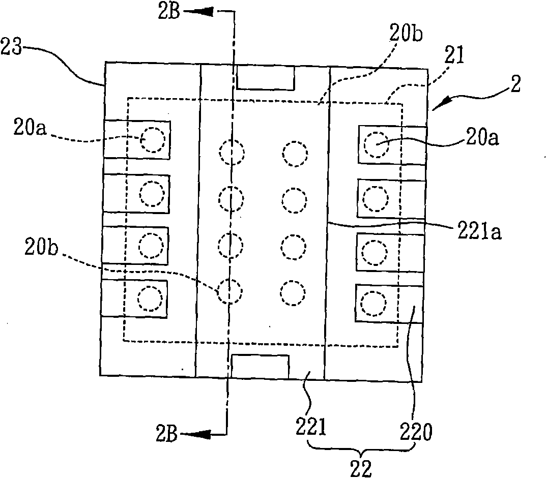
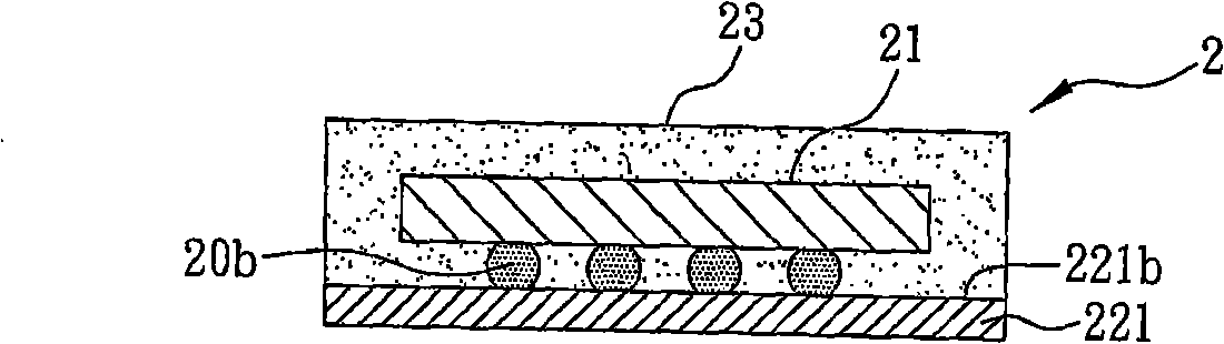
[0075] like Figure 4A and Figure 4B Shown is a top view and an edge view of a semiconductor package according to a second embodiment of the present invention Figure 4A A cross-sectional view taken along line 4B-4B.

[0076] As shown in the figure, the semiconductor package 4 of the second embodiment is substantially the same as that described in the first embodiment. , the slit 421a is non-linear, so that the formation of the zigzag slit 421a provides a bonding area between the ground plane 421 and the encapsulant 43, thereby further improving the bonding between the ground plane 421 and the encapsulant 43; And the formation position of the zigzag slit 421 a is not located in the middle of the ground plane 421 , so that the formation position of the slit is not limited.

[0077] In order to further enhance the bonding between the ground plane 421 and the encapsulation body 43, recesses 421f and 421g can be formed on both sides of the ground plane 421 along the longitudin...


PUM


Abstract

The invention discloses a flip chip semiconductor encapsulating part which takes a lead frame as a chip bearing part and comprises a chip electrically connected to the lead frame by solder bumps in a flip chip way, and an molding colloid which encapsulates the chip, the solder bumps and the lead frame, wherein, the lead frame is composed of a plurality of leads and a ground plane positioned among the leads, a slit is formed on the ground plane, a molding compound used for forming the molding colloid can be filled in the slit, thereby the associativity between the ground plane and the molding colloid is promoted and the relamination of the junction surface between the ground plane and the molding colloid in the subsequent temperature cycle can be avoided so as to enhance the dependability of the finished product.

Description

technical field [0001] The invention relates to a flip-chip semiconductor package technology, in particular to a flip-chip semiconductor package with a lead frame as a chip carrier and the applied lead frame. Background technique [0002] The traditional FCQFN (Flip Chip Quad Flat Non-Leaded) semiconductor package is as follows figure 1 In the shown structure, a chip 11 is placed on a lead frame 12 through a plurality of solder bumps 10 in a flip-chip manner, so that the chip 11 and the lead frame 12 form an electrical connection relationship; the chip 11, the lead frame 12 and solder bumps 10 are coated with an encapsulant 13, and after the encapsulant 13 is formed, the side surfaces (SideSurface) 120a and bottom surface (Bottom Surface) 120b (Bottom Surface) 120b of each lead 120 of the lead frame 12 are exposed. The encapsulant 13, and make the bottom surface 120b of each lead 120 flush with the bottom surface 13b of the encapsulant 13, so that the guide pin 120 of the p...

Claims


Application Information

Patent Timeline
Patent Type & Authority Applications(China)
IPC IPC(8): H01L23/488H01L23/495H01L23/31
CPCH01L2224/16245
Inventor 吕维隆林志男邱世冠陈锦德
Owner SILICONWARE PRECISION IND CO LTD
Features
  • R&D
  • Intellectual Property
  • Life Sciences
  • Materials
  • Tech Scout
  • Unparalleled Data Quality
  • Higher Quality Content
  • 60% Fewer Hallucinations
Learn More