Optical power detection apparatus and method

A technology of optical power detection and power, which is applied in the field of optical communication, can solve problems such as the inability to make good use of digital amplifiers, narrow detection range, and low voltage resolution, so as to facilitate debugging and fault location, improve sampling accuracy, and ensure reliability Effect

Inactive Publication Date: 2008-11-05
ZTE CORP
0 Cites 6 Cited by

AI-Extracted Technical Summary

Problems solved by technology

However, due to its uniform resolution, the current ADC generally only has an input detection range of 2.5V, so the voltage resolution per dB is too low, which affects the detection accuracy of optical power, resulting in some Applications requiring precision detection cannot make good use of the advantages of logarithmic amplif...

Method used

As can be seen from above-mentioned embodiment, because the technical solution of the present invention has adopted logarithmic amplifier, thereby guaranteed detection range is big, has solved the unbalanced problem of detection resolution in the whole detection range, simultaneously, the technical solution The optical power sampling circuit introduces the subtraction circuit part, so that the sampling accuracy is greatly improved. At the same time, the composition of the circuit is relatively simple, which is convenient for debu...

Abstract

The invention discloses an optical power detecting device and method, pertaining to the optical communication field. The method of the invention includes: after the photoelectric conversion of the light to be measured, executing subtraction arithmetic to the output voltage magnitude of the light to be measured and the known voltage magnitude, to obtain a difference value; amplifying the difference value, and combining the known voltage magnitude to calculate for obtaining the optical power of the light to be measured. The technical scheme of the invention greatly improves the sampling accuracy, simultaneously has relative simple circuit structure, which is convenient for debugging and fault locating; in addition, the technical scheme of the invention remarkably improves the power testing accuracy and ensures the optical power testing reliability.

Application Domain

Technology Topic

Image

  • Optical power detection apparatus and method
  • Optical power detection apparatus and method

Examples

  • Experimental program(2)
  • Effect test(1)

Example Embodiment

[0038] Example 1
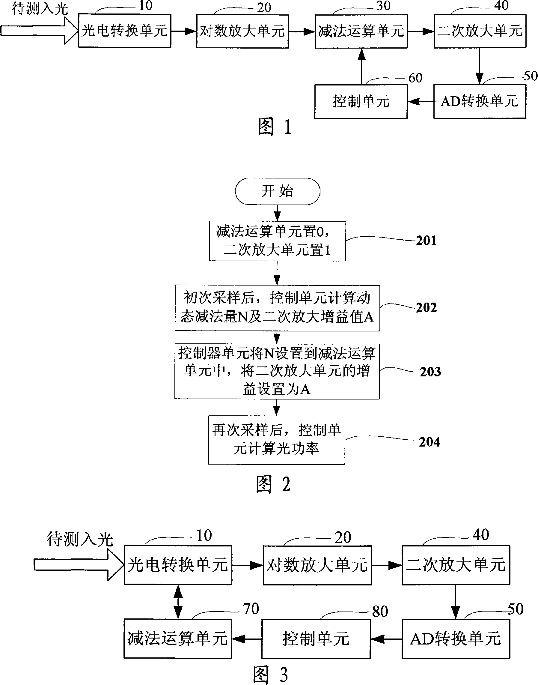
[0039] A high-precision optical power detection device, as shown in Figure 1, includes a photoelectric conversion unit (10), a logarithmic amplification unit (20), a subtraction unit (30), and a secondary amplification unit (40) connected in sequence, wherein The subtraction unit (30) is also connected to the control unit (60), the secondary amplifying unit (40) is connected to the AD (analog to digital) conversion unit (50), and the control unit (60) is connected to the AD conversion unit (50). The following is a detailed introduction to the functions of each unit.
[0040] The photoelectric conversion unit (10) is used for photoelectric conversion, and can adopt APD or PIN conversion circuit;
[0041] The logarithmic amplification unit (20) is used to logarithmically amplify the voltage output result of the photoelectric conversion;
[0042] The subtraction operation unit (30) performs subtraction operation on the voltage output result of the logarithmic amplifying unit (20) according to the control of the control unit (60), which can be realized by an integrated operation circuit. In this embodiment, the subtraction operation unit also has a built-in There is an AD conversion function module and a digital interface. The control unit sends a dynamic subtraction value N to the subtraction unit through the data interface, and the subtraction unit performs AD conversion on the N value to realize the subtraction operation of the voltage output result;
[0043] In other embodiments, the AD conversion function module can also be placed outside the subtraction unit or the AD conversion unit (50) in the device can be used. At this time, the control unit performs AD conversion on the dynamic subtraction value N first. And then sent to the subtraction unit.
[0044] The secondary amplification unit (40) performs secondary amplification on the output result of the subtraction operation unit (30), which can be realized by using an integrated operational amplifier;
[0045] The AD conversion unit (50) performs AD sampling on the voltage output result of the secondary amplifying unit (40), which can be realized by an ADC chip;
[0046] The control unit (60) controls the execution of AD sampling, feedback calculation and optical power calculation, wherein the dynamic subtraction amount N and the secondary amplification gain value are obtained through the feedback calculation, and the optical power is calculated by the re-sampling value, the dynamic subtraction amount N and the calibration coefficient. Power, the unit can be implemented based on MCU (Micro Controller Unit, Micro Controller Unit) or FPGA (Field Programmable Gate Array).
[0047]In the normal working process of the above device, the user determines the detection resolution M (unit can be dB) according to the needs, then performs AD sampling, and calculates the appropriate secondary amplification gain A and dynamic subtraction N according to the sampling results. Set to the subtraction unit, after A is set to the secondary amplifying unit, perform AD sampling again, and then calculate the optical power. The specific process, as shown in Figure 2, includes the following steps:
[0048] Step 201: The control unit sets the subtraction unit to zero, and sets the gain of the secondary amplifying unit to 1;
[0049] Step 202: The control unit controls the AD conversion unit to perform the first AD sampling on the voltage after photoelectric conversion through logarithmic amplification, and after converting the current sampling voltage value, calculate the corresponding dynamic subtraction amount according to the required detection resolution M N (the unit can be mV or uA), and the gain value A of the secondary amplifying unit;
[0050] In this step, the control unit calculates the values ​​of N and A according to the following formula:
[0051] Secondary amplification gain value A≥(V ref /Nda)/(M×K) formula (1)
[0052] Among them, M is the detection resolution, in this embodiment, M=0.01dBm; K is the output slope of the logarithmic amplifier, in this embodiment K=40mV/dB; Vref is the reference source of the AD conversion unit, and the common one is 2.5V , Namely 2500mV; Nda is the full scale of the AD conversion unit, and the full scale of the 10-bit AD conversion unit is 2 10 =1024;
[0053] After substituting the above-mentioned parameter values ​​into formula (1) for calculation,
[0054] A≥(2500/1024)/(0.01×40)=6.1, so A is set to 7 in this embodiment.
[0055] After the secondary amplification, the voltage entering the AD conversion unit cannot exceed its reference voltage V ref , Therefore:
[0056] (V in -N)×A≤V ref , That is, N≥V in -V ref -/A formula (2)
[0057] Where V in It is the voltage value of AD sampling when the gain value of the secondary amplification is 1, so N≥V in -357mV.
[0058] Step 203: The control unit sets the above-mentioned dynamic subtraction amount N to the input end of the subtraction unit, and sets the gain of the secondary amplifying unit to A;
[0059] In other embodiments, the control unit may first convert the dynamic subtraction quantity N into an analog quantity through an AD conversion function module, and then send it to the subtraction unit.
[0060] Step 204: The control unit controls the AD conversion unit again, performs AD sampling on the voltage values ​​sequentially through logarithmic amplification, subtraction, and secondary amplification after photoelectric conversion, and calculates the optical power according to the calibration coefficient and the dynamic subtraction amount N.
[0061] In other embodiments, after the initial sampling is completed, the optical power can be detected in real time, that is, multiple AD samplings can be performed to calculate the optical power in real time. In each process of detecting the optical power, the control unit needs to be based on the previous AD sampling. The result of re-determining the dynamic subtraction value N.

Example Embodiment

[0062] Example 2
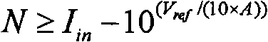
[0063] The optical power detection device provided by this embodiment is shown in Figure 3. The device includes a photoelectric conversion unit (10), a logarithmic amplification unit (20), a secondary amplification unit (40), and an AD conversion unit (50) connected in sequence. ), a control unit (80) and a subtraction unit (70), wherein the photoelectric conversion unit (10) is also connected to the subtraction unit (70). The following is a detailed introduction to the functions of each unit.
[0064] The photoelectric conversion unit (10) is used for photoelectric conversion, and can adopt APD or PIN conversion circuit;
[0065] The logarithmic amplification unit (20) is used to logarithmically amplify the shunted circuit voltage;
[0066] The subtraction unit (70) can be realized by using a controllable current source to divide a part of the current from the PD circuit, and this part of the current can be converted into a voltage value. In this embodiment, the subtraction unit also has a built-in AD conversion function Module, and a digital interface, the control unit sends a dynamic subtraction value N to the subtraction unit through the data interface, and the subtraction unit performs AD conversion on the N value to realize the subtraction operation on the current output result of the photoelectric conversion;
[0067] In other embodiments, the AD conversion function module can also be placed outside the subtraction unit or the AD conversion unit (50) in the device can be used. At this time, the control unit performs AD conversion on the dynamic subtraction value N first. And then sent to the subtraction unit.
[0068] The secondary amplifying unit (40) realizes the adjustment and amplification of the output voltage of the previous stage, which can be realized by using an integrated operational amplifier;
[0069] In other embodiments, the logarithmic amplifying unit and the secondary amplifying unit can also be combined into one amplifying unit, that is, after the PD circuit is shunted, it can be amplified once.
[0070] The AD conversion unit (50) performs AD sampling on the output result of the secondary amplifying unit (40) and sends it to the control unit, which can be realized by an ADC chip;
[0071] The control unit (80) controls the execution of AD sampling, feedback calculation and optical power calculation, wherein the dynamic subtraction amount N and the secondary amplification gain value are obtained through the feedback calculation, and the voltage and fixed value corresponding to the re-sampling value and the dynamic subtraction amount N are obtained through the feedback calculation. Calculate the optical power based on standard coefficients. The unit can be implemented based on MCU or FPGA.

PUM

no PUM

Description & Claims & Application Information

We can also present the details of the Description, Claims and Application information to help users get a comprehensive understanding of the technical details of the patent, such as background art, summary of invention, brief description of drawings, description of embodiments, and other original content. On the other hand, users can also determine the specific scope of protection of the technology through the list of claims; as well as understand the changes in the life cycle of the technology with the presentation of the patent timeline. Login to view more.

Similar technology patents

Analog accelerometer output signal transmission device

InactiveCN103389091AImprove sampling accuracySolve the problem of easy introduction of electromagnetic interference signalsNavigation by speed/acceleration measurementsVIT signalsEngineering
Owner:西安应用光学研究所

Method and apparatus for identifying high-risk commodities by sampling inspection

InactiveCN109146585AReduce sampling costImprove sampling accuracyBuying/selling/leasing transactionsLimit valueComputer science
Owner:BEIJING JINGDONG SHANGKE INFORMATION TECH CO LTD +1

Classification and recommendation of technical efficacy words

  • Simple composition
  • Improve sampling accuracy

Method for controlling mobile robot on basis of hand signals

ActiveCN102789327ASimple compositionHelp to carryInput/output processes for data processingMobile robotMobile robot control
Owner:合肥欣奕华智能机器股份有限公司

Human energy metabolism detection device and method

InactiveCN104665835AImprove sampling accuracyThe sampling process is uninterruptedDiagnostic recording/measuringSensorsCarbon dioxide sensorThrottle
Owner:HEFEI INSTITUTES OF PHYSICAL SCIENCE - CHINESE ACAD OF SCI +1

Solid recorder for posture measuring

InactiveCN101261748AImprove sampling accuracySampling rate adjustableRegistering/indicating working of vehiclesSolid state recorderLinear acceleration
Owner:ZHONGBEI UNIV
Why Eureka
Try Eureka