Photolithography process including a chemical rinse

A lithography process, semiconductor technology, applied in the field of lithography process

Active Publication Date: 2008-11-12
TAIWAN SEMICON MFG CO LTD
View PDF0 Cites 5 Cited by
  • Summary
  • Abstract
  • Description
  • Claims
  • Application Information

AI Technical Summary

Problems solved by technology

[0005] The technical problem to be solved by the present invention is to provide a method for performing a photolithography process with a chemical cleaning step and a method for semiconductor manufacturing, so as to solve the water mark caused by the cleaning step in the photolithography process and improve the patterned photoresist structure Problems with line edge roughness

Method used


Image

  • Photolithography process including a chemical rinse
  • Photolithography process including a chemical rinse
  • Photolithography process including a chemical rinse

Examples


Embodiment Construction

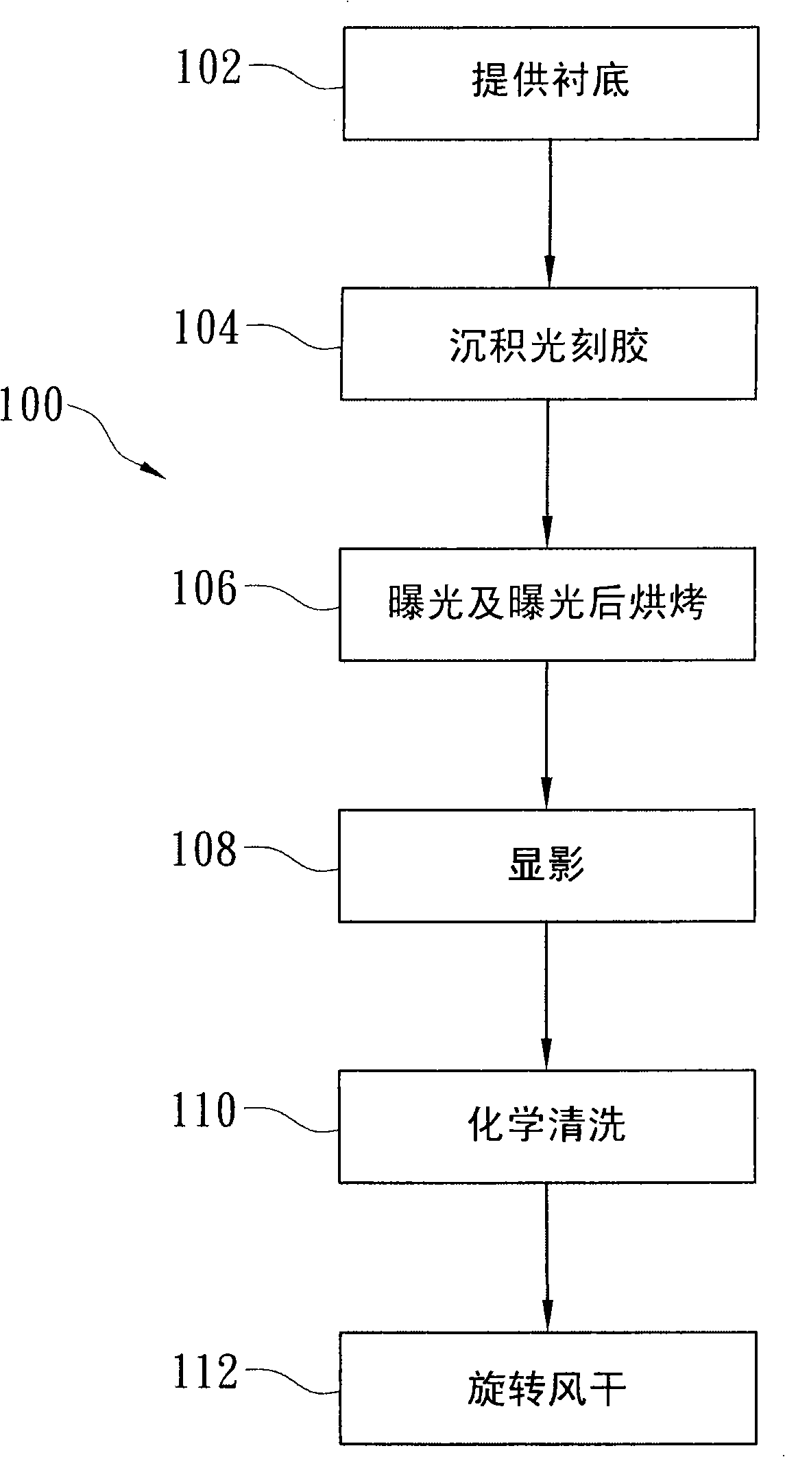
[0027] The present invention relates to a method of manufacturing a semiconductor device, and in particular to a photolithography process with a chemical cleaning process. It should be understood that the specific embodiments hereinafter are presented to illustrate the concept of the invention and enable those skilled in the art to practice the invention. In addition, it should also be understood that the operating methods and devices disclosed in the embodiments of the present invention may include certain known processes or structures. When these known structures or processes are mentioned in the embodiments, the descriptions of their detailed parts are only for general discussion. In addition, repeated use of the same reference number for the same device in the drawings is for convenience of description, rather than representing any combination of structures or steps in the drawings.

[0028] figure 1 A flowchart of a photolithography process method 100 according to an em...


PUM


Abstract

The present disclosure provides a plurality of methods of performing a lithography process. In one embodiment, a substrate including a layer of photoresist is provided. The layer of photoresist is exposed. The exposed layer of photoresist is developed. A chemical rinse solution is applied to the developed photoresist. The chemical rinse solution includes an alcohol base chemical. The substrate is spun dry.

Description

technical field [0001] The invention relates to a photolithography process used to manufacture semiconductor integrated circuits, and in particular to a method for carrying out the photolithography process with chemical cleaning steps and a semiconductor manufacturing method. Background technique [0002] Photolithography is a technique for projectively transferring a pattern on a mask onto a substrate such as a semiconductor wafer. The semiconductor photolithography technology includes covering a photoresist layer on the surface of a semiconductor substrate and exposing the photoresist layer to form a pattern. A post-exposure bake process (post-exposure bake; PEB) is usually used to break the polymer structure of the photoresist after exposure. Then the substrate is sent into the developing reaction chamber, the surface of the substrate contains interrupted polymer photoresist, and the photoresist material dissolved in the aqueous developing solution is removed in the reac...

Claims


Application Information

Patent Timeline
Patent Type & Authority Applications(China)
IPC IPC(8): H01L21/027G03F7/26G03F7/30
CPCG03F7/40G03F7/38
Inventor 张庆裕林进祥
Owner TAIWAN SEMICON MFG CO LTD
Why Eureka
Try Eureka