Offset calibration methods and radio frequency data path circuits

一种校准方法、校准电路的技术,应用在电气元件、数字传输系统、头的配置/安装等方向,能够解决信号数据分割层误判、数据读取质量不佳等问题

Inactive Publication Date: 2008-11-19
MEDIATEK INC
View PDF0 Cites 2 Cited by
  • Summary
  • Abstract
  • Description
  • Claims
  • Application Information

AI Technical Summary

Problems solved by technology

[0005] In order to solve the problem of poor data reading quality caused by the bias voltage generated in the radio frequency data path circuit in the prior art, which leads to misjudgment of the signal data segmentation layer or the cut-off of the saturated part of the signal, the present invention provides a bias calibration Method and RF Datapath Offset Calibration Circuit

Method used


Image

  • Offset calibration methods and radio frequency data path circuits
  • Offset calibration methods and radio frequency data path circuits
  • Offset calibration methods and radio frequency data path circuits

Examples


Embodiment Construction

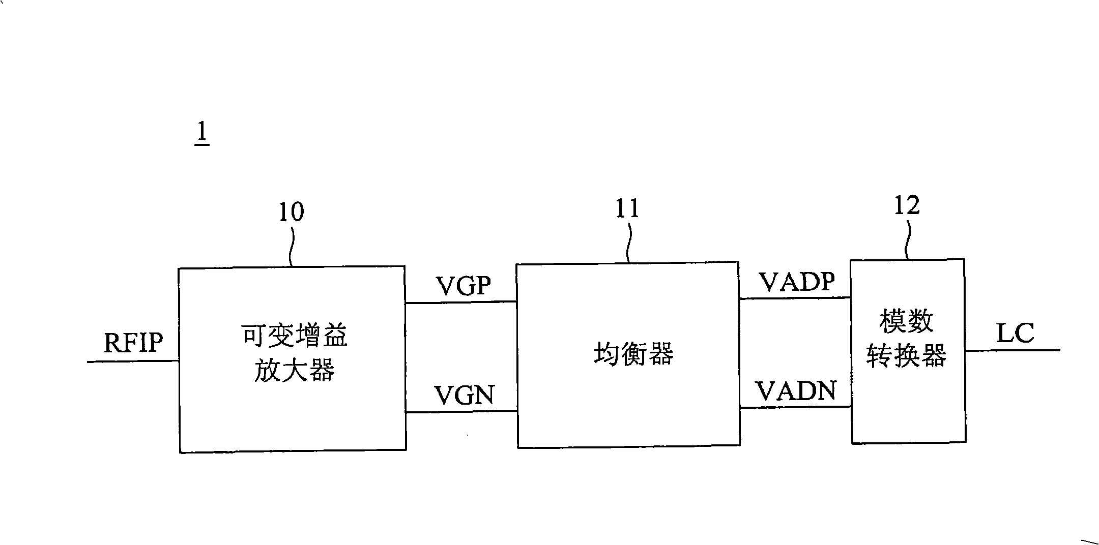
[0018] FIG. 4 is a schematic diagram of an embodiment of a radio frequency data path offset calibration circuit according to the present invention. The RF data path offset calibration circuit 4 includes an amplifier 40 , an equalizer 41 , an analog-to-digital converter 42 , an offset calibration unit 43 , an offset calibration unit 44 and a determination unit 45 . The amplifier 40 (such as a variable gain amplifier) ​​at least includes an input terminal IN40, output terminals OUT40a and OUT40b. At least one input terminal IN40 of the amplifier 40 receives the input signal RFIP, and the signal RFIP is the sum of the data signal A, the signal B, the signal C, and the signal D read by the optical read-write head, or the input terminal IN40 of the amplifier 40 is directly received by The data signal A, signal B, signal C, or signal D read by the optical read / write head. In the normal mode, the amplifier 40 generates the gain signal VGP and the signal VGN according to the input si...


PUM


Abstract

The invention provides an offset calibration method and an offset calibration circuit with the radio frequency data path. The method comprises: two input terminals of an equalizer are switched to a common voltage at a first time point, wherein the equalizer generates a first equalized signal and a second equalized signal according to the common voltage. It is determined whether a first offset voltage is present in the equalizer according to the first and second equalized signals generated from the common voltage. If the first offset voltage is determined to be present in the equalizer, a first compensation voltage is provided to the equalizer. The offset calibration method and the offset calibration circuit with the radio frequency data path of the invention can eliminate the offset voltage of the radio frequency data path and enhance the data reading quality via processing the offset calibration for two phases of the radio frequency data path.

Description

technical field [0001] The present invention relates to an offset calibration method, in particular to an offset calibration of a radio frequency (RFradio frequency) data path circuit, in particular to an offset calibration method and a radio frequency data path offset calibration circuit. Background technique [0002] figure 1 It is a schematic diagram of an existing radio frequency data path circuit. Such as figure 1 As shown, the radio frequency data path circuit 1 includes a variable-gain amplifier (variable-gain amplifier VGA) 10 , an equalizer (equalizer) 11 and an analog-to-digital converter (analog-to-digital converter ADC) 12 . The variable gain amplifier 10 receives a signal RFIP, which is the sum of a data signal A, a signal B, a signal C, a signal D and a reference signal read by an optical pickup head. The variable gain amplifier 10 generates and transmits the signal VGP and the signal VGN to the equalizer 11 . The equalizer 11 generates a signal VADP and a ...

Claims


Application Information

Patent Timeline
Patent Type & Authority Applications(China)
IPC IPC(8): G11B7/09
CPCH04L25/061H04L27/01
Inventor 陈建铭黄志坚林尚毅
Owner MEDIATEK INC
Why Eureka
Try Eureka