
Semiconductor testing apparatus and semiconductor memory testing method

A test device and semiconductor technology, applied in the direction of static memory, read-only memory, information storage, etc., can solve the problems of time-consuming, increased test time, increased test cost, etc., and achieve the effect of shortening the test time

Inactive Publication Date: 2008-11-26
ADVANTEST CORP
View PDF0 Cites 9 Cited by
  • Summary
  • Abstract
  • Description
  • Claims
  • Application Information

AI Technical Summary

Problems solved by technology

[0004] However, although writing to a bad block and comparison of the resulting signals are prohibited, access to each page within the bad block is still performed
Each access time is shorter than the usual test time for a good block, but quite time consuming since the access is performed for each page within a bad block
[0005] In particular, the capacity of NAND-type flash memory has doubled every year in recent years, so the test time associated with this has also tended to increase
So, accessing unwanted bad blocks will result in increased test cost

Method used


Image

  • Semiconductor testing apparatus and semiconductor memory testing method
  • Semiconductor testing apparatus and semiconductor memory testing method
  • Semiconductor testing apparatus and semiconductor memory testing method

Examples


Embodiment Construction

[0019] Hereinafter, embodiments of the present invention will be described with reference to the drawings. This embodiment is not intended to limit the present invention.

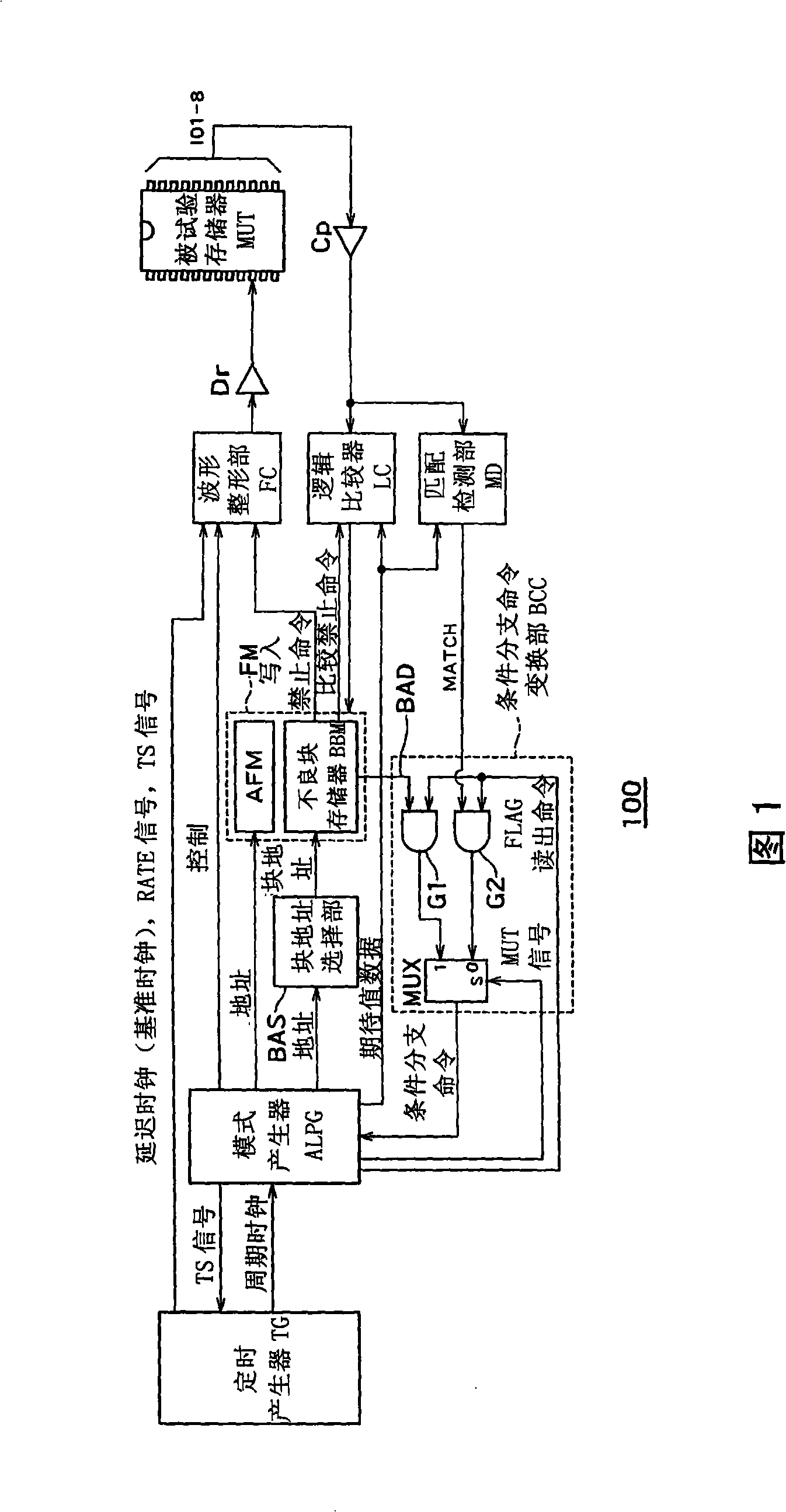
[0020] FIG. 1 is a schematic block diagram of a semiconductor memory testing device 100 (hereinafter referred to as device 100 ) according to an embodiment of the present invention. The device 100 includes: a timing generator TG, a pattern generator ALPG, a waveform shaper FC, a logic comparator LC, a fail bit memory FM, a block address selection unit BAS, a match detection unit MD, and a conditional branch command change unit BCC.

[0021] The pattern generator ALPG outputs a timing setting signal (TS signal) to the timing generator TG. The timing generator TG receives the TS signal, and generates timing edges of various channels defined based on the timing settings described in the device test program. Thus, the timing generator TG generates a periodic clock and a delayed clock. The pattern generator A...


PUM


Abstract

A testing apparatus for testing a tested memory having a block function that can rewrite data for each of blocks each consisting of a plurality of pages each consisting of a plurality of bits. The testing apparatus comprises a pattern generating part (ALPG) that produces the address information of a page and generates a testing pattern; a waveform shaping part (FC) that shapes the testing pattern to output a testing signal based on the testing pattern; a comparing part (LC) that compares a resultant signal outputted by the tested memory with an expected value; and a bad block memory (BBM) that stores information of faulty blocks of the tested memory in advance and that, if the page specified by the address information is included in a faulty block, outputs a faulty signal to be used for skipping from that address information to the address information of a page included in a tested block next to the faulty block.

Description

technical field [0001] The present invention relates to a semiconductor test device, for example, to a semiconductor test device for testing a data storage type memory rewritable in blocks such as a NAND flash memory. Background technique [0002] The semiconductor memory test device includes: a timing generator, a pattern generator, a waveform shaper and a logic comparator. The timing generator generates a periodic clock and a delay clock based on timing data designated by a timing setting signal (hereinafter referred to as a TS signal) output from the pattern generator. The pattern generator outputs the test pattern data given to the memory under test (MUT (Memory Under Tester)) according to the periodic clock from the timing generator. The test mode data is given to the waveform shaper, and the waveform shaper uses the delayed clock to shape the waveform at the timing required for the test, and applies the shaped test signal to the memory under test. The resulting signa...

Claims


Application Information

Patent Timeline
Patent Type & Authority Applications(China)
IPC IPC(8): G11C29/56G01R31/28
CPCG11C29/56G11C29/56004G11C16/06G11C16/08G11C29/00
Inventor 佐藤新哉太幡诚
Owner ADVANTEST CORP
Learn More