Fully differential comparator and fully differential amplifier

A technology of amplifying circuits and differential amplifiers, which is applied to electric pulse generator circuits, amplifiers using switched capacitors, multiple input and output pulse circuits, etc. High-quality fully differential analog signal processing, improved offset reduction effect

Inactive Publication Date: 2008-11-26
PANASONIC CORP
View PDF3 Cites 11 Cited by
  • Summary
  • Abstract
  • Description
  • Claims
  • Application Information

AI Technical Summary

Problems solved by technology

In addition, when comparing a differential input signal that is very close to the differential comparison reference voltage, there are also problems such as charge injection at the time of switch switching for charge storage in

Method used


Image

  • Fully differential comparator and fully differential amplifier
  • Fully differential comparator and fully differential amplifier
  • Fully differential comparator and fully differential amplifier

Examples


Embodiment Construction

[0056] Hereinafter, embodiments of the present invention will be described with reference to the drawings.

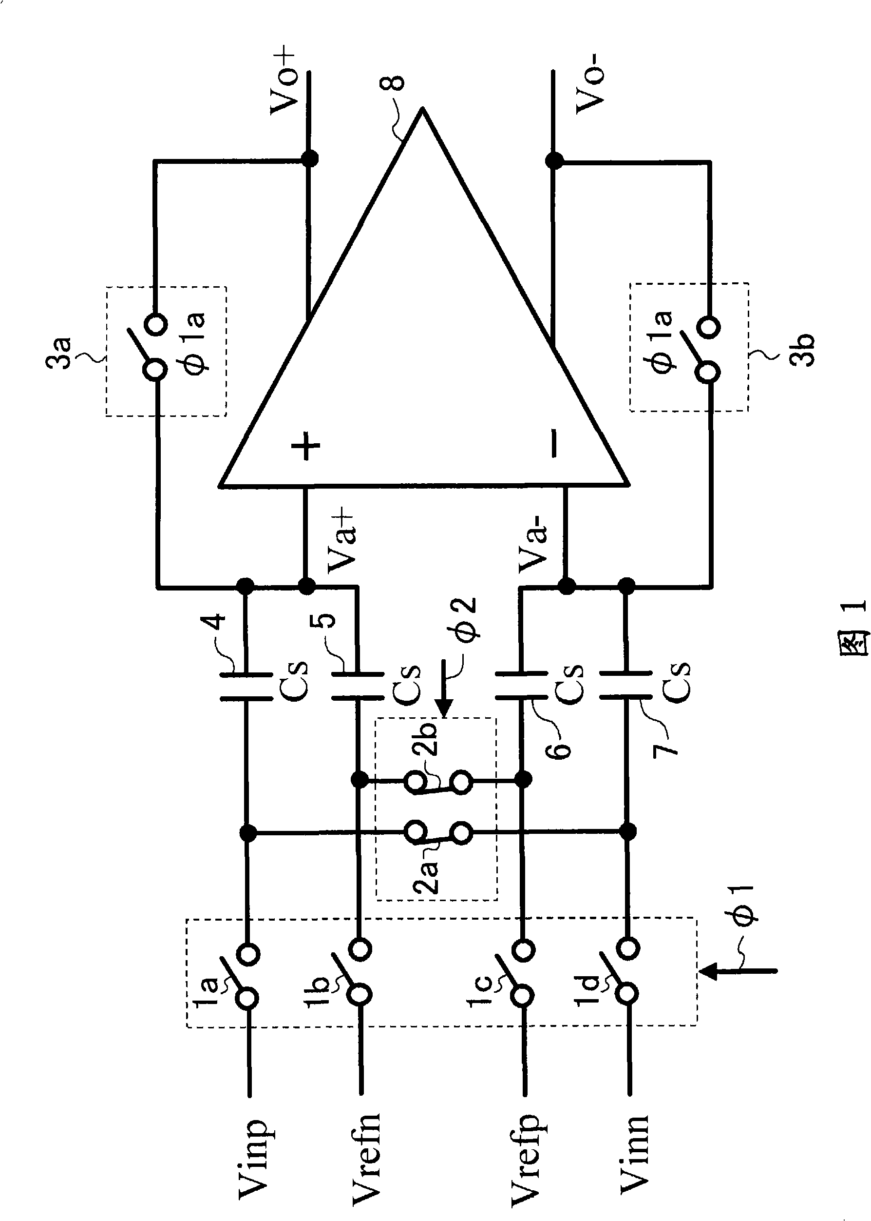
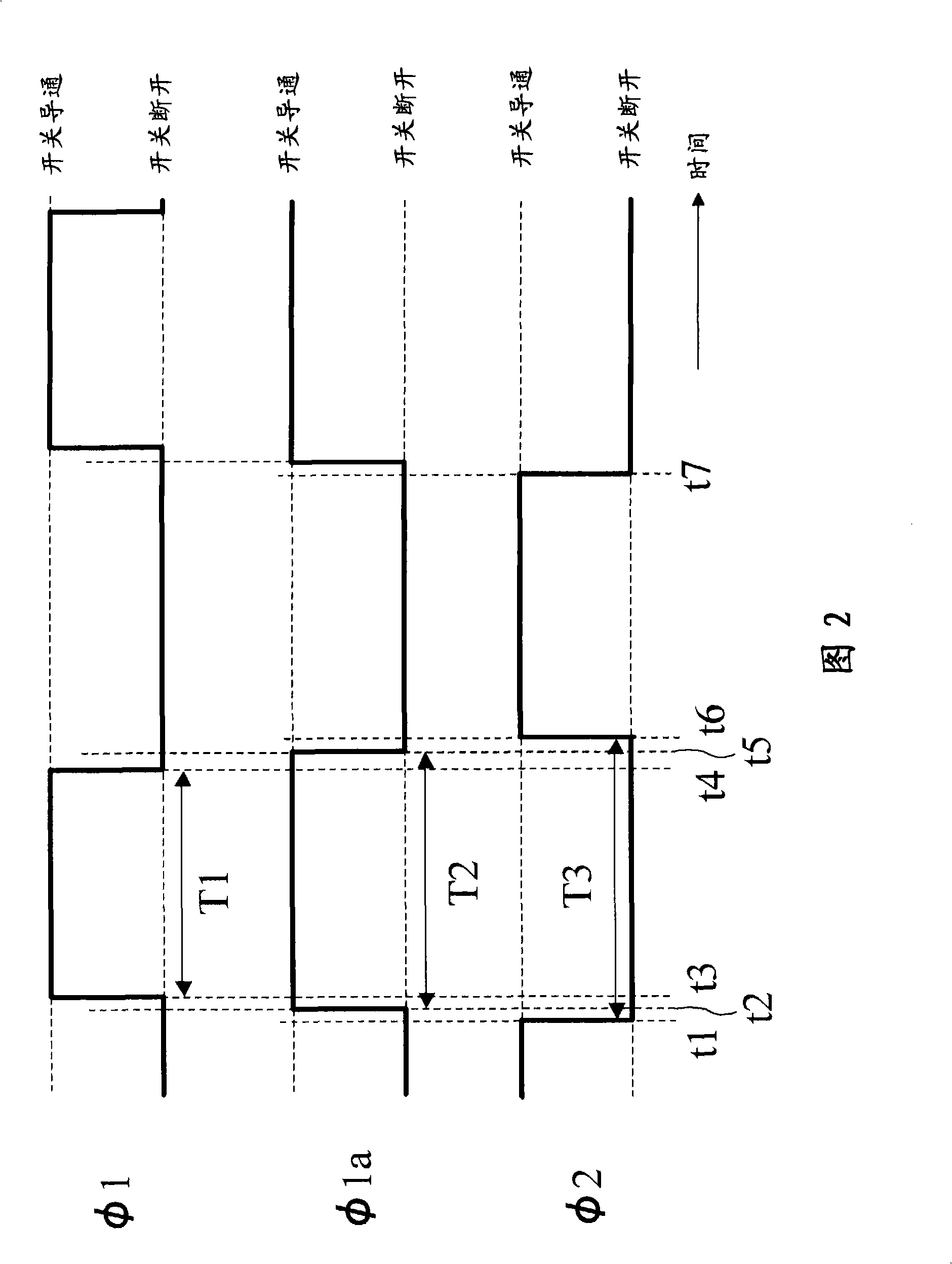
[0057] FIG. 1 shows a configuration example of a fully differential comparator according to the present invention. In Fig. 1, 1a, 1b, 1c, 1d are the first to fourth sampling switches, 2a, 2b are the first charge redistribution switch and the second charge redistribution switch, 3a, 3b are the first reset switch and the second Reset switch, 4, 5, 6, 7 are first to fourth sampling capacitors, 8 is a differential amplifier. In addition, Vinp and Vinn are differential input signal voltages, Vrefp and Vrefn are differential comparison reference voltages, Va+ and Va- are positive and negative polarity input terminals of the differential amplifier 8, and Vo+ and Vo- are differential amplifier 8 input terminals. Positive and negative polarity output terminals. The first to fourth sampling capacitors 4 to 7 substantially have the same capacitance value Cs. Φ1, Φ1a, and Φ2 are...


PUM


Abstract

A first to a fourth sampling switch (1a to 1d), a first to a fourth sampling capacitor (4 to 7), and a first and a second charge redistribution switch (2a, 2b) are provided on the input side of a differential amplifier (8). A first and a second reset switch (3a, 3b) are provided between the input and the output of the differential amplifier (8). An input signal voltage (Vinp) having a positive polarity, a comparison reference voltage (Vrefn) having a negative polarity, a comparison reference voltage (Vrefp) having a positive polarity, and an input signal voltage (Vinn) having a negative polarity are respectively applied through a first to a fourth sampling switch (1a to 1d) to one end of each of the first to the fourth sampling capacitor (4 to 7). During a reset period, the reset of the differential amplifier (8) is released after sampling of each voltage is completed, and during a comparison period, the first and the second charge redistribution switch (2a, 2b) are electrically connected.

Description

technical field [0001] The invention relates to a technology capable of realizing high-precision comparison and high-precision amplification of differential input signals under the condition of high-speed operation and low power consumption in a fully differential analog signal processing circuit with a large dynamic range. Background technique [0002] In recent years, there has been an increasing demand for lower voltage, higher speed, and lower power consumption of analog signal processing circuits. For this reason, recently, technologies using a switched capacitor structure combining an amplifier and a capacitor of a CMOS analog circuit, which can secure a dynamic range under low power supply voltage conditions and realize high-speed operation, are becoming mainstream. [0003] On the other hand, from the viewpoint of the interface technology between analog and digital, general-purpose ADC (analog-to-digital converter) resolution improvement and high-speed performance ar...

Claims


Application Information

Patent Timeline
IPC IPC(8): H03K5/08H03M1/12
CPCH03M1/1245H03F3/005H03F3/45475H03F3/45968H03F2203/45134H03F2203/45212H03K5/2481H03K5/249H03K5/22H03M1/12H03K3/45
Inventor 樋口真浩
Owner PANASONIC CORP
Why Eureka
Try Eureka