Double gate manufactured with locos techniques

一种栅极、厚氧化层的技术,应用在半导体功率器件领域,达到消除回侵现象、改进灵活性、减少Ciss的效果

Active Publication Date: 2008-12-10
ALPHA AND OMEGA SEMICONDUCTOR (CAYMAN) LIMITED
View PDF0 Cites 7 Cited by
  • Summary
  • Abstract
  • Description
  • Claims
  • Application Information

AI Technical Summary

Problems solved by technology

These technical problems and performance limitations are generally exacerbated when the cell density increases due to the reduction in the size of the trench opening when trench power devices are formed on semiconductor substrates

Method used


Image

  • Double gate manufactured with locos techniques
  • Double gate manufactured with locos techniques
  • Double gate manufactured with locos techniques

Examples


Embodiment Construction

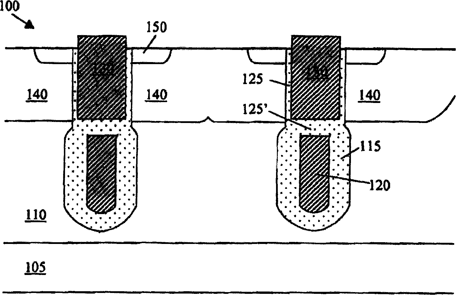
[0032] The following will refer to the attached figure 2 ~ Accompanying drawing 3 describes the present invention in detail.

[0033] refer to figure 2 Shown is a schematic cross-sectional view of the trench MOSFET device 100 of the present invention. Trench MOSFET device 100 is supported on substrate 105 on which epitaxial layer 110 is formed. Trench MOSFET device 100 includes a bottom gate segment 120 below a top trench gate segment 130 , the bottom of which is filled with polysilicon. The polysilicon-filled bottom gate segment 120 is shielded and insulated from the top gate polysilicon segment 130 by an insulating oxide layer 125' disposed between the top and bottom segments. The bottom channel segment is also insulated from the drain disposed below 105 by an insulating layer 115 surrounding the bottom surface of the trench gate. The top trench gate segment 130 is also polysilicon filled at the top of the trench surrounded by a gate insulating layer 125 covering ...


PUM


Abstract

This invention discloses a trenched semiconductor power device that includes a trenched gate surrounded by a source region encompassed in a body region above a drain region disposed on a bottom surface of a substrate. The trenched gate further includes at least two mutually insulated trench-filling segments with a bottom insulation layer surrounding a bottom trench-filling segment having a bird-beak shaped layer on a top portion of the bottom insulation attached to sidewalls of the trench extending above a top surface of the bottom trench-filling segment.

Description

technical field [0001] The present invention mainly relates to semiconductor power devices, and more specifically, relates to an improved and novel manufacturing process and device structure of a semiconductor device with a double-gate structure provided by applying LOCOS (Local Oxidation of Silicon, local oxidation of silicon) technology . Background technique [0002] Currently, conventional techniques for reducing gate-drain capacitance in DMOS (double-diffused metal-oxide-semiconductor) devices using discrete trench gates such as shielded gate trench (SGT) structures still face many technical limitations and difficulties. Specifically, trenched DMOS devices have a trenched gate in their structure, where the large capacitance (Cgd) between the gate and drain limits the switching speed of the device. This capacitance is mainly due to the electric field coupling between the bottom of the trench gate and the drain. To reduce the gate-to-drain capacitance, an improved discr...

Claims


Application Information

Patent Timeline
Patent Type & Authority Applications(China)
IPC IPC(8): H01L29/78H01L29/423H01L27/088H01L21/336H01L21/28H01L21/8234
CPCH01L29/407H01L29/42368H01L29/66734H01L29/7813
Inventor 戴嵩山胡永中
Owner ALPHA AND OMEGA SEMICONDUCTOR (CAYMAN) LIMITED
Why Eureka
Try Eureka