Supercharge Your Innovation With Domain-Expert AI Agents!

Assistance processing method for printed circuit board

A printed circuit board and auxiliary processing technology, which is applied to the formation of electrical connection of printed elements and the formation of conductive patterns, etc., can solve the problems of easy breakage and open circuit of ink, increased ink loss, and exposed copper, so as to save material cost investment and improve The effect of work efficiency

Inactive Publication Date: 2008-12-24
靖江市杰华网络技术有限公司
View PDF0 Cites 12 Cited by
  • Summary
  • Abstract
  • Description
  • Claims
  • Application Information

AI Technical Summary

Problems solved by technology

The situation in Figure C is unqualified. If it is used as a solder resist ink, if the ink at the hole is too thin or even there is no copper exposure in the subsequent electroplating process, if it is used as a conductive ink, the ink at the hole is too thin. , in the subsequent baking process or in the environmental test process, the ink here is very easy to break and cause poor open circuit
The situation in Figure C is a problem that is often encountered in the printing process of flexible boards. If it is not dealt with during the printing process, it will directly affect the final quality of the board.
[0005] When the flexible circuit board prints ink on the through hole, it usually adopts some auxiliary processing methods to ensure the reliability of the ink on the through hole. The board is directly placed on the table and fixed by vacuum adsorption, but due to the existence of air pressure, the ink at the orifice will be too thin. At this time, it is necessary to increase the number of printings to increase the printing thickness to ensure the thickness of the ink at the orifice. The board needs to be printed two to three times; the specific operation steps of the printing method of the flexible printed circuit board with PET as the base material are as follows: (1) Cut the PET film to the processing size → (2) Drill holes → (3) Clean → ( 4) To be printed → (5) Vacuuming → (6) Print the conductive silver paste on the PET and scrape once → (7) Scratch the second time → (8) Transfer the printed PET film to the baking rack to wait Baking → (9) Wipe the silver paste on the printing table with alcohol → (10) Baking the silver paste → (11) Collect the PET board → (12) Repeat the above operation to print the silver paste line on the second side, but this kind of direct In order to ensure the ink thickness of the orifice, the printing method must be scraped two to three times, which directly causes a waste of silver paste; and each time a sheet is printed, the countertop must be wiped, which not only delays the working time but also causes the silver paste to be wiped dirty. The hidden danger of polluting the next PET film; although this method is common in the current flexible board printing process, it also has its own shortcomings that cannot be ignored: repeated printing is required, wasting man-hours, and the amount of ink loss is also increased. The most serious thing is that the ink leaks directly onto the operation table during printing, and the table needs to be wiped every time after printing, and the work efficiency is too low

Method used


Image

  • Assistance processing method for printed circuit board
  • Assistance processing method for printed circuit board
  • Assistance processing method for printed circuit board

Examples


Embodiment Construction

[0032] A preferred embodiment of an auxiliary processing method for a printed circuit board of the present invention, the steps of which include:

[0033] (1) Cutting, making the base material of the circuit board to be processed into a processing size;

[0034] (2) Drilling, setting up positioning holes on the base material of the circuit board to be processed;

[0035] (3) Cleaning, washing the processed circuit board base material with water, and then drying;

[0036] (4) to be printed;

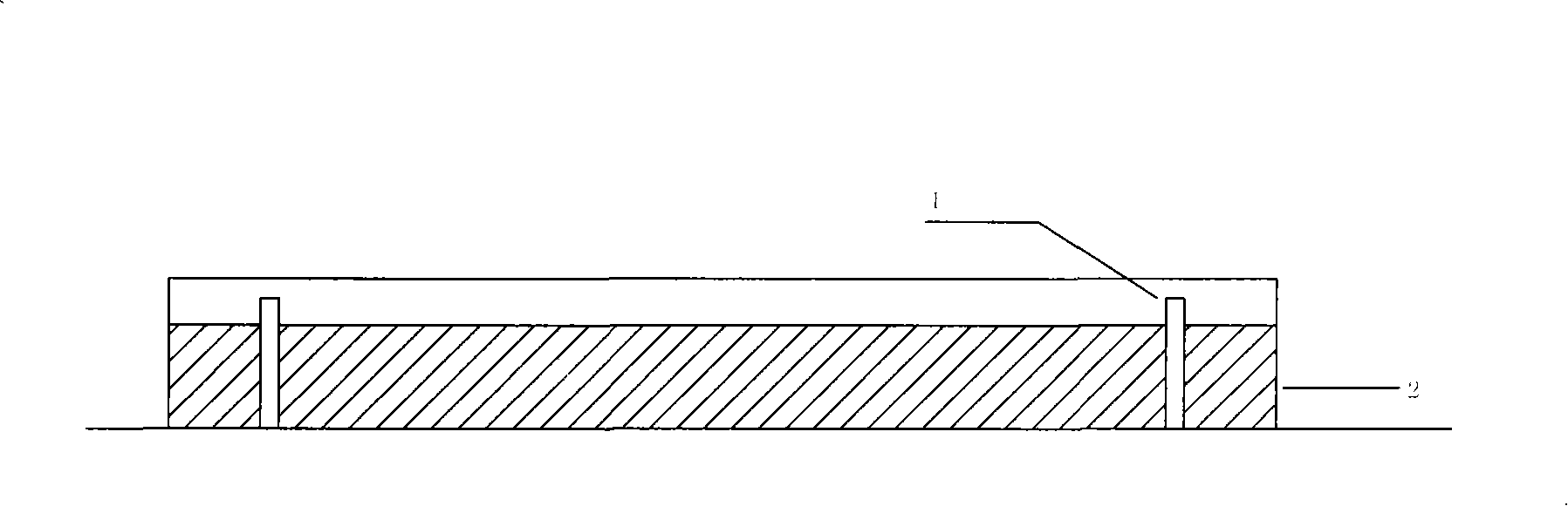
[0037] (5) Paste a layer of medium on the back of the printed surface of the circuit board substrate to be processed;

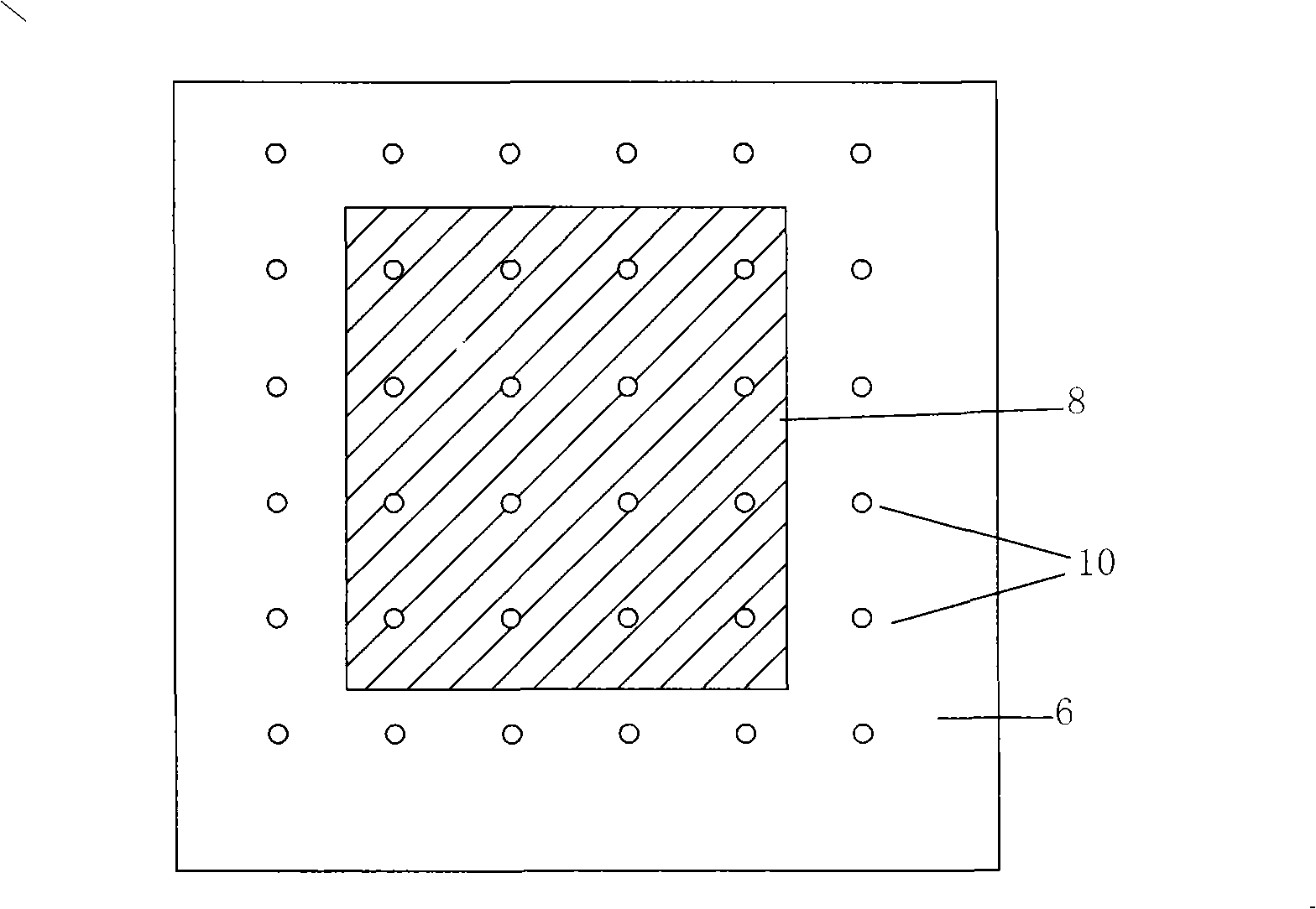
[0038] The medium used in the step (5) is newsprint; the step (5) includes the following steps: ① cutting the medium into the processing size; ② drilling holes in the medium; ③ using the drilled medium as a liner Material pads on the printing table, such as Figure 4 In the step of the drilling shown in the figure: the medium is drilled to form an avoidance hole 7, th...


PUM


Abstract

The invention relates to an auxiliary processing method for a printed circuit board, and comprises the following steps: (1) cutting; (2) drilling; (3) cleaning; (4) being ready for printing; (5) pumping vacuum; (6) printing conductive silver paste on the circuit board to be processed; (7) collecting the circuit board to be processed; (8) printing a silver paste circuit on a second surface through repeating the operations. The auxiliary processing method further comprises the following step between step (4) and step (5): a layer of medium is stuck at the back of the surface to be printed of the substrate of the circuit board to be processed, and further comprises the following step between step (6) and step (7): the medium is taken out. By adopting the auxiliary processing method, the operating efficiency is enhanced, and the invested material cost is saved.

Description

technical field [0001] The invention relates to a method for manufacturing a printed circuit board, in particular to an auxiliary processing method for a printed circuit board suitable for ink printing in a vacuum adsorption manner. Background technique [0002] With the development of electronic products in the direction of high density, miniaturization and high reliability, the printed circuit boards supporting electronic products are also gradually developing in the direction of lightness, thinness and flexibility. Among them, the flexible printed circuit board (FPC) has been more and more widely used in electronic products due to its advantages of bending, folding, three-dimensional wiring, and three-dimensional space interconnection, and has replaced the traditional rigid printed circuit board ( PCB). [0003] In the general concept, the circuit board referred to by flexible printed circuit board (FPC) is mainly a circuit board made of PI film as the base material and ...

Claims


Application Information

Patent Timeline
Patent Type & Authority Applications(China)
IPC IPC(8): H05K3/40H05K3/12
Inventor 李贤维
Owner 靖江市杰华网络技术有限公司
Features
  • R&D
  • Intellectual Property
  • Life Sciences
  • Materials
  • Tech Scout
  • Unparalleled Data Quality
  • Higher Quality Content
  • 60% Fewer Hallucinations
Learn More