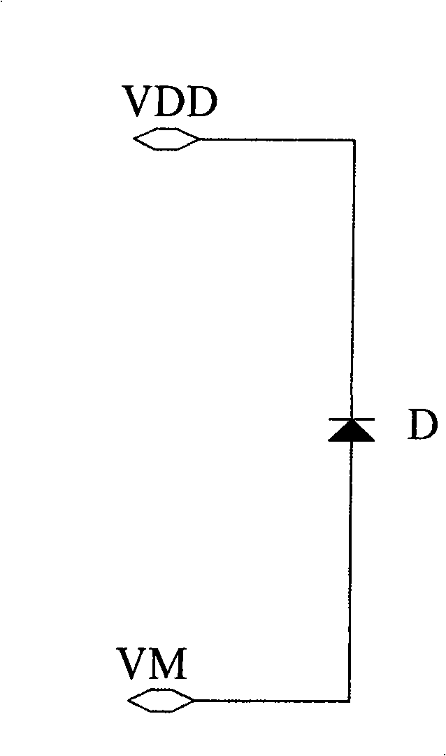
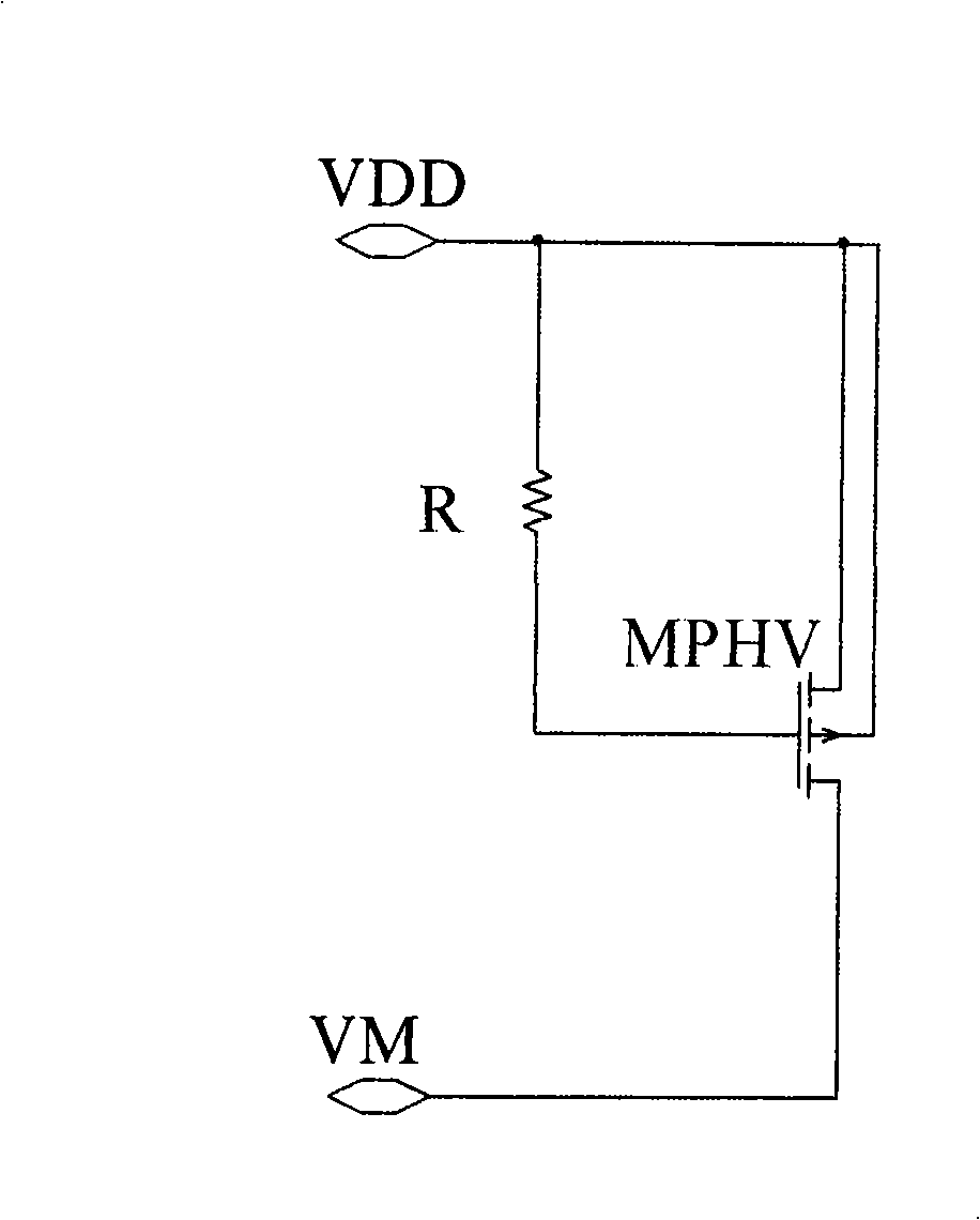
Electrostatic discharging protection circuit
An electrostatic discharge protection and circuit technology, applied in emergency protection circuit devices, emergency protection circuit devices for limiting overcurrent/overvoltage, circuits, etc. Problems such as poor ability to discharge current
- Summary
- Abstract
- Description
- Claims
- Application Information
AI Technical Summary
Problems solved by technology
Method used
Image

Examples
Embodiment Construction
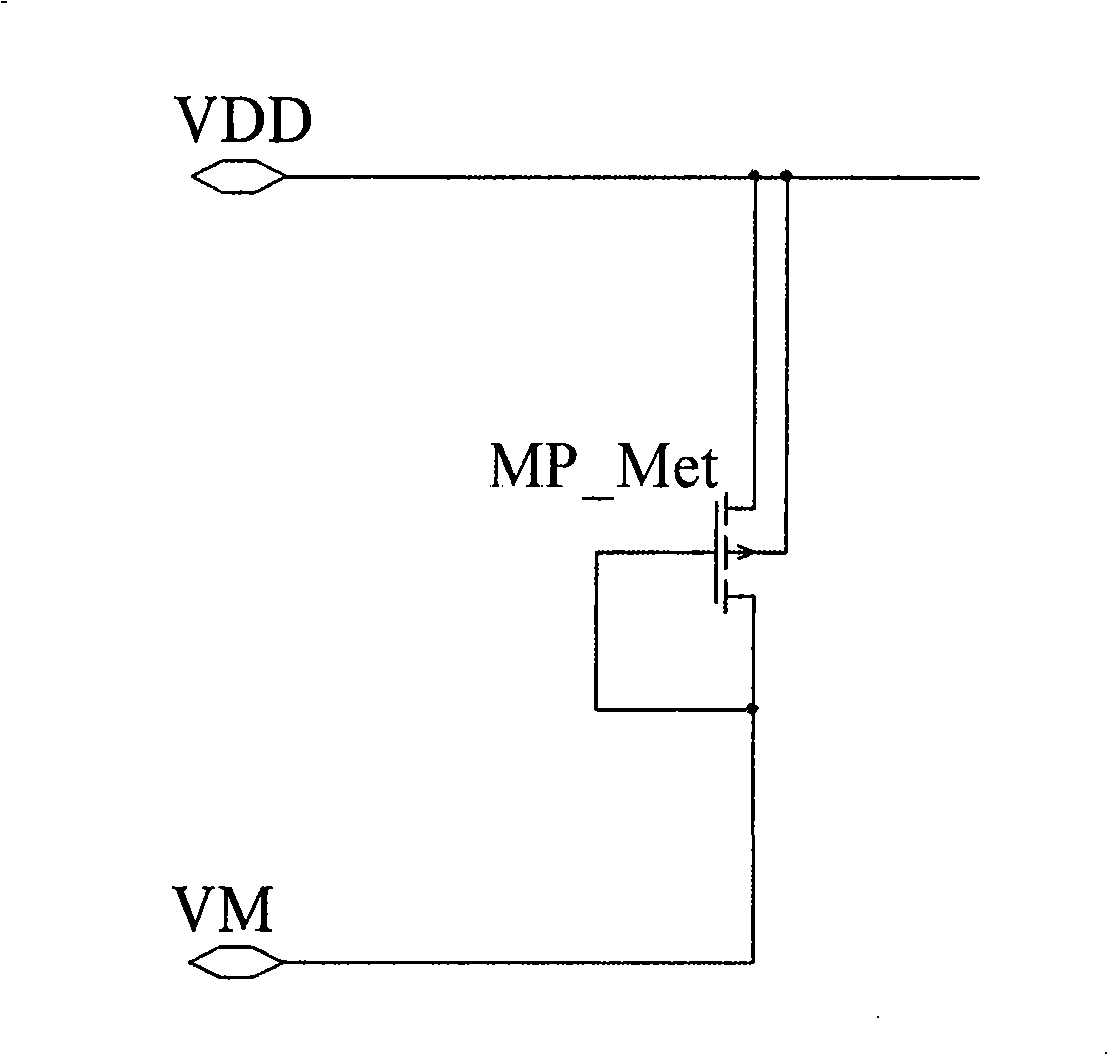
[0023] image 3 It is an electrostatic protection circuit using parasitic PMOS in high voltage process.
[0024] Such as image 3 As shown, the drain of the PMOS is connected to the gate and is connected to the VM terminal, and the source is connected to the substrate and is connected to the VDD terminal.
[0025] Figure 4 yes image 3 Physical cross-section of the PMOS shown.
[0026] Such as Figure 4 As shown, the gate of this parasitic PMOS is formed of metal, and between the metal gate and the channel is field oxide, generally referred to as field oxide. Generally, the turn-on voltage of the parasitic PMOS with the bottom metal (generally called Met1 in the process) as the gate is about -35V. Of course, the threshold voltage can be properly adjusted according to design requirements, mainly by modifying the thickness of the field oxide layer between the metal gate and the channel. For example, in order to obtain a higher turn-on threshold voltage, a higher metal la...
PUM
 Abstract
Description
Claims
Application Information
 - R&D
- Intellectual Property
- Life Sciences
- Materials
- Tech Scout
- Unparalleled Data Quality
- Higher Quality Content
- 60% Fewer Hallucinations
Browse by: Latest US Patents, China's latest patents, Technical Efficacy Thesaurus, Application Domain, Technology Topic, Popular Technical Reports.
© 2025 PatSnap. All rights reserved.Legal|Privacy policy|Modern Slavery Act Transparency Statement|Sitemap|About US| Contact US: help@patsnap.com