Output circuit for FPGA clock signal and processing method thereof

A clock signal output, clock signal technology, applied in logic circuits using specific components, logic circuits using basic logic circuit components, etc., can solve problems such as amplitude changes, other signal phase shifts, FPGA clock tree collapse, etc. achieve the effect of reducing lag

Inactive Publication Date: 2009-01-28
VIMICRO CORP
View PDF0 Cites 8 Cited by
  • Summary
  • Abstract
  • Description
  • Claims
  • Application Information

AI Technical Summary

Problems solved by technology

In such a processing circuit and method, the clock signal output by the BUFG not only enters the clock terminal of the flip-flop, but also passes through the common logic unit. Therefore, the clock tree after the BUFG has a relatively large delay; moreover, the output clock s

Method used


Image

  • Output circuit for FPGA clock signal and processing method thereof
  • Output circuit for FPGA clock signal and processing method thereof
  • Output circuit for FPGA clock signal and processing method thereof

Examples


Embodiment Construction

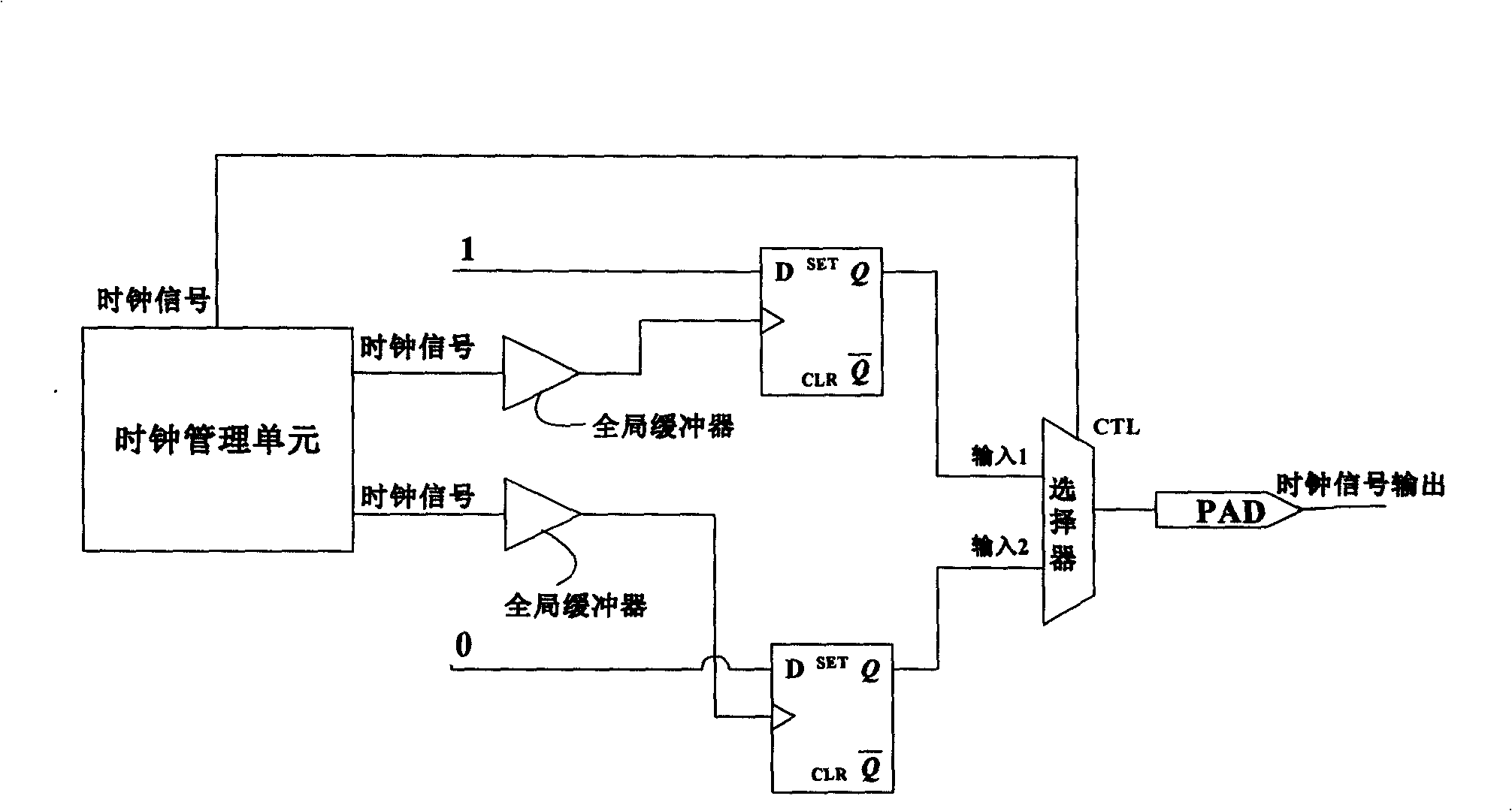
[0021] figure 1 It is the FPGA clock non-phase output circuit diagram using two flip-flops of the present invention. As shown in the figure, in this kind of circuit, the flip-flop unit is composed of two D flip-flops in parallel.

[0022] The clock management unit of the FPGA generates and outputs a clock signal, which enters the clock terminals of the two D flip-flops through the global buffer BUFG. Since the clock signal output by the FPGA needs to be in phase with its internal clock signal, that is, the so-called positive phase output, the input signal of a D flip-flop is connected to logic "1", and its output terminal is connected to the first input signal terminal of the selector; The input signal of a D flip-flop is connected to logic "0", and its output terminal is connected to the second input signal terminal of the selector.

[0023] The control signal of the selector is the clock signal output by the clock management unit. When it is "1", the first input signal ou...


PUM


Abstract

The invention discloses an FPGA clock signal output circuit, comprising a clock management unit and a global buffer, wherein a clock signal generated by the clock management unit is distributed by the global buffer; moreover, the FPGA clock signal output circuit also comprises a trigger unit and a selector, the end of the clock signal of the trigger unit is connected with the output end of the global buffer, a data input signal of the trigger unit is a constant logic signal, the trigger unit provides a positive output signal and a negative output signal to the end of the input signal of the selector, the control input end of the selector is connected with the end of the clock signal outputted by the clock management unit, and the selector outputs the clock signal to an output pin of the FPGA. The FPGA clock signal outputted by the circuit reduces the delay, and lowers the negative influence of the external load on an internal clock tree of the FPGA.

Description

technical field [0001] The invention relates to an FPGA clock signal output circuit. Background technique [0002] In modern integrated circuit design, the use of FPGA is becoming more and more common, especially in the field of ASIC design and application. FPGA can not only complete the prototype verification in the ASIC design process, but also directly play the role of ASIC in the relatively simple ASIC design. [0003] For the FPGA system, whether it is used for prototype verification or directly used as an ASIC, it is often necessary to output clock signals to peripheral devices, such as SDRAM clocks, LCD clocks, and camera clocks. However, due to the particularity of the FPGA production process, the wiring between the internal components has been completely fixed before leaving the factory, and the clock tree structure has been pre-cured in the FPGA chip; Therefore, FPGA cannot solve the clock skew problem by dynamically building a clock buffer tree like ASIC. In add...

Claims


Application Information

Patent Timeline
IPC IPC(8): H03K19/173
Inventor 邹杨
Owner VIMICRO CORP
Why Eureka
Try Eureka