Nonvolatile memory and forming method for the same

A non-volatile memory technology, applied in the manufacture of electrical solid-state devices, semiconductor devices, semiconductor/solid-state devices, etc., can solve the problems of low charge storage capacity, high charge loss capacity, poor charge capture ability, etc., to reduce Thermal budget, best programmatic effect

Active Publication Date: 2009-02-11
MACRONIX INT CO LTD
View PDF0 Cites 8 Cited by
  • Summary
  • Abstract
  • Description
  • Claims
  • Application Information

AI Technical Summary

Problems solved by technology

[0005] However, for silicon nitride as the material of the nitride layer in SONOS, if it is a silicon nitride film rich in nitrogen, it is mostly a deep-level charge storage center, and the ability of charge trapping is compared to shallow-level defects. co

Method used


Image

  • Nonvolatile memory and forming method for the same
  • Nonvolatile memory and forming method for the same
  • Nonvolatile memory and forming method for the same

Examples


Example Embodiment

[0040] In order to make the above and other objects, features and advantages of the present invention more comprehensible, preferred embodiments are specifically cited below and described in detail with accompanying drawings.

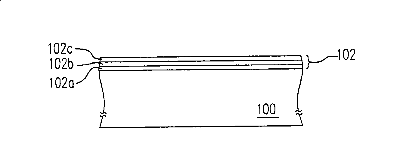
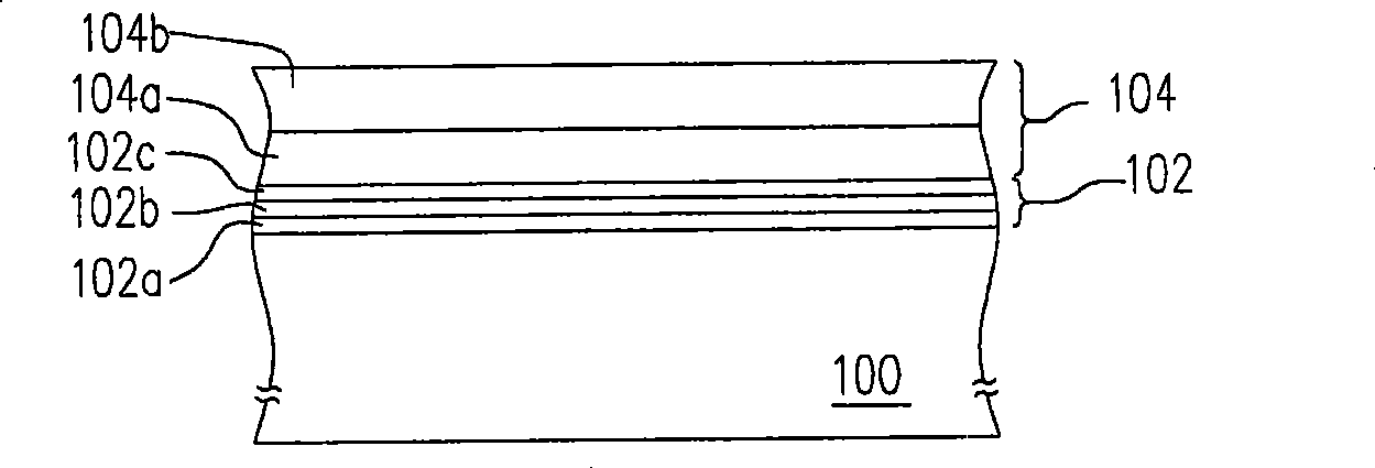
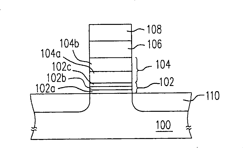
[0041] Figure 1A to Figure 1C Illustrated is a method for forming a non-volatile memory according to a preferred embodiment of the present invention. First please refer to Figure 1A , providing a substrate 100 , and then forming a tunneling layer 102 on the substrate 100 . The tunneling layer 102 can be a dielectric layer with a single-layer structure, and the material of the dielectric layer is, for example, silicon oxide or other dielectric materials with high dielectric constant. The methods for forming the single-structure dielectric layer include chemical vapor deposition, rapid high-temperature process, and ion oxidation process. In this embodiment, the tunneling layer 102, such as Figure 1AAs shown, it has a multi-layer structure, and its f...


PUM

PropertyMeasurementUnit
Thicknessaaaaaaaaaa

Abstract

The invention provides a nonvolatile memory, which is positioned on a substrate and comprises a tunneling layer, a charge capture composite layer, a grid and a source electrode/drain electrode area, wherein, the tunneling layer is positioned on the substrate; the charge capture composite layer is positioned on the tunneling layer; the grid is positioned above the charge capture composite layer; and the source electrode/drain electrode area is positioned in the substrate on both sides of the tunneling layer. The nonvolatile memory provided with the charge capture composite layer has good programming and erasing performance and data retaining capability. In addition, the high thermal budget technology is not needed for the formation of the charge capture composite layer, thereby reducing the thermal budget during the technological process.

Description

technical field [0001] The present invention relates to a non-volatile memory component and its manufacturing method, and in particular to a non-volatile memory with a multi-layer charge trapping layer and its manufacturing method. Background technique [0002] Known electrically programmable and erasable non-volatile memory technologies based on charge storage structures, such as electrically erasable programmable read-only memory (EEPROM) and flash memory, are used in a variety of modern applications. [0003] As the size of integrated circuits shrinks, there is increasing interest in charge trapping layer based memory cell structures because of the scalability and ease of the fabrication process. Memory cell structures based on charge trapping layers include those known (for example) by the industry names Nitride ROM, Silicon-Oxide-Nitride-Oxide-Silicon (SONOS) and Band Engineered Silicon-Oxide-Nitride -Oxide-silicon (BE-SONOS) and other structures. These memory cell st...

Claims


Application Information

Patent Timeline
IPC IPC(8): H01L29/792H01L29/51H01L27/115H01L21/336H01L21/28H01L21/8247
Inventor 王嗣裕吕函庭
Owner MACRONIX INT CO LTD
Why Eureka
Try Eureka