Formation method and etching method for amorphous carbon hard mask layer

A hard mask layer, amorphous carbon technology, applied in electrical components, semiconductor/solid-state device manufacturing, circuits, etc., can solve high thermal budget, affect device stability, and uneven thickness uniformity of amorphous carbon hard mask layer Good and other issues, to achieve the effect of maintaining consistency

Active Publication Date: 2013-06-05
SEMICON MFG INT (SHANGHAI) CORP
View PDF6 Cites 7 Cited by
  • Summary
  • Abstract
  • Description
  • Claims
  • Application Information

AI Technical Summary

Problems solved by technology

[0004] The existing amorphous carbon hard mask layer is formed by plasma-enhanced chemical vapor deposition (PECVD), and a high temperature of 400 to 600 degrees Celsius is used in the process of forming the amorphous carbon hard mask layer by the plasma-enhanced chemical vapor deposition process. The thickness uniformity of the amorphous carbon hard mask layer formed at the existing high temperature is not good, and the thermal budget is high, which affects the stability of the device

Method used


Image

  • Formation method and etching method for amorphous carbon hard mask layer
  • Formation method and etching method for amorphous carbon hard mask layer
  • Formation method and etching method for amorphous carbon hard mask layer

Examples


Embodiment Construction

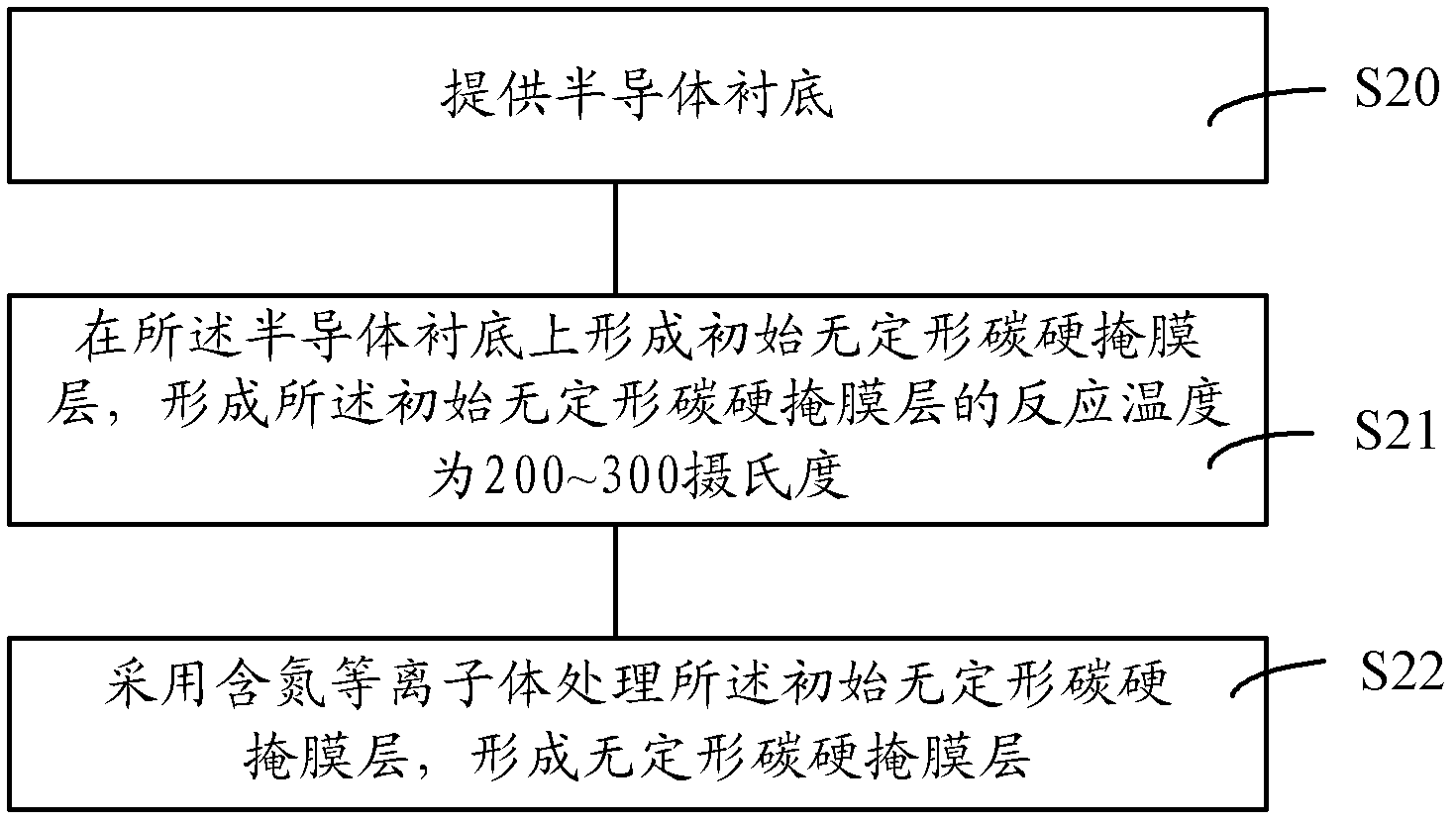
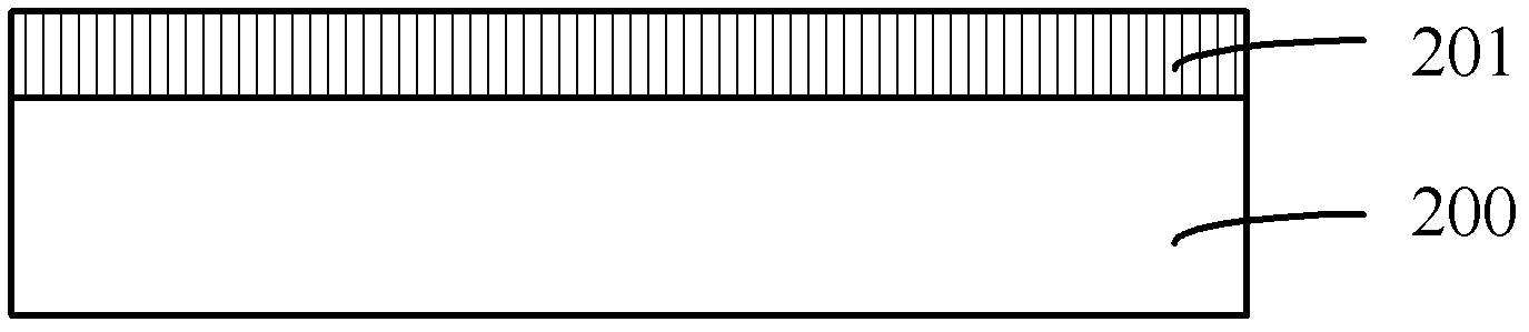
[0038] The inventor found in the process of making the amorphous carbon hard mask layer that when the amorphous carbon hard mask layer is formed by the existing plasma enhanced chemical vapor deposition process (PECVD), due to the high temperature of 400-600 degrees Celsius, Higher temperature affects the distribution and activity of dopant ions in the substrate or (polysilicon) POLY. The higher the temperature, the more serious the effect, which increases the thermal budget for making the amorphous carbon hard mask layer, and the formation of high temperature without The uniformity of the thickness of the shaped carbon hard mask layer is not good. When the photoresist layer is subsequently formed on the amorphous carbon hard mask layer, the uniformity of the thickness of the photoresist layer is affected, and abnormal photolithographic patterns are formed after exposure and development. , reducing the stability of the device.

[0039] In order to reduce the thermal budget, th...


PUM


Abstract

Provided is a formation method for an amorphous carbon hard mask layer. The formation method includes that a semiconductor substrate is provided; the initial amorphous carbon hard mask layer is formed on the semiconductor substrate and a reaction temperature for the formation of the initial amorphous carbon hard mask layer is 200 DEG C-300 DEG C; nitrogenous plasma is used for processing the initial amorphous carbon hard mask layer. The formation method of the amorphous carbon hard mask layer forms the amorphous carbon hard mask layer by adopting a low temperature technology, the amorphous carbon hard mask layer with high compactness is formed by the method that the nitrogenous plasma is used for processing the initial amorphous carbon hard mask layer, the heating budget is reduced and stability of a device is improved.

Description

technical field [0001] The invention relates to the field of semiconductor manufacturing, in particular to a method for forming an amorphous carbon hard mask layer and an etching method. Background technique [0002] The manufacture of semiconductor integrated circuits uses a series of processes such as lithography, etching, implantation and deposition to form a large number of various types of complex devices on the same silicon substrate, and interconnect them to have complete electronic functions. With the rapid development of ultra-large-scale integrated circuits, the integration of chips is getting higher and higher, and the size of components is getting smaller and smaller. The various effects caused by the high density and small size of devices have an increasingly prominent. [0003] Taking hard mask technology as an example, when the semiconductor process enters 90nm, due to the smaller and smaller photolithography size, it is often necessary to form a hard mask la...

Claims


Application Information

Patent Timeline
Patent Type & Authority Applications(China)
IPC IPC(8): H01L21/033H01L21/027H01L21/308
Inventor 张彬邓浩
Owner SEMICON MFG INT (SHANGHAI) CORP
Why Eureka
Try Eureka