

Manufacture method of HD Ru nanocrystalline atomic layer deposition for flash memory
An atomic layer deposition and memory technology, which is used in semiconductor/solid-state device manufacturing, semiconductor devices, electrical components, etc., and can solve the problems of lack of metal layer thickness and poor spatial controllability.
- Summary
- Abstract
- Description
- Claims
- Application Information
AI Technical Summary
Problems solved by technology
Method used
Image

Examples
Embodiment 1
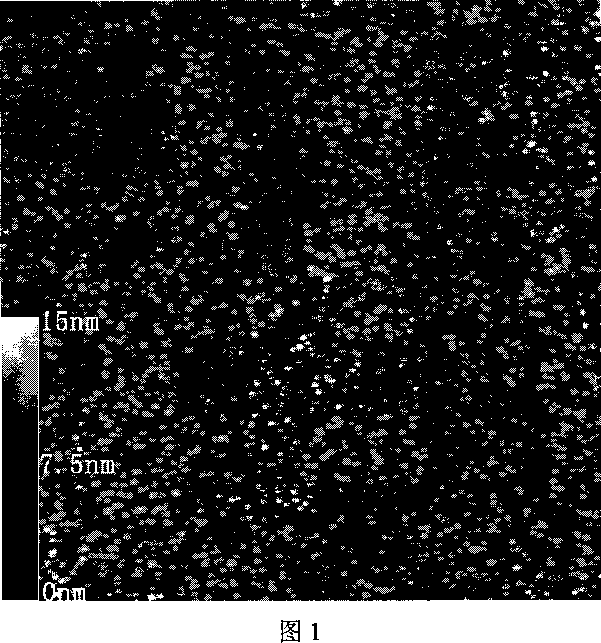
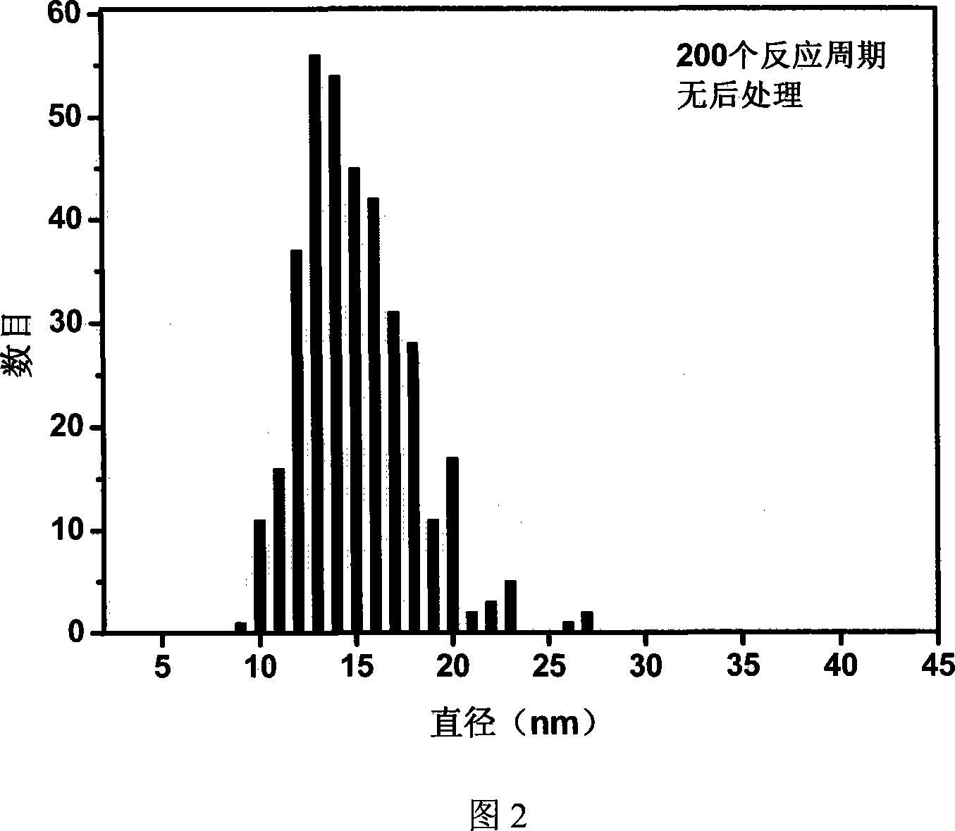
[0027] After cleaning the silicon wafer by traditional process, grow 3nm high dielectric constant Al by atomic layer deposition method 2 o 3 For thin films, the reaction sources used are trimethylaluminum and water. Then, with dicycloyl ruthenium (RuCp 2 ) and oxygen as the reaction source, using the atomic layer deposition method on Al 2 o 3 Ru nanocrystals are deposited on the film. The substrate temperature used in this example is 330°C, the pressure in the reaction chamber is about 2.5 Torr, the number of ALD reaction cycles is 200, and a single reaction cycle includes 2 seconds of RuCp 2 Carrier gas is introduced, nitrogen is purged for 2 seconds, oxygen is introduced for 1 second, and nitrogen is purged for 2 seconds. The obtained Ru nanocrystals have an average diameter of 14 nm and a density of 9 × 10 10 cm -2 ,as shown in picture 2. Table 2 lists the effects of different annealing conditions on the size and density of Ru nanocrystals. It can be seen that the s...
PUM
 Abstract
Description
Claims
Application Information