Method for forming and processing high-K gate dielectric layer and method for forming transistor

A gate dielectric layer and transistor technology, applied in the fields of forming, forming transistors, and processing high-K gate dielectric layers, can solve the problems of increased thermal budget of semiconductor devices, long time, local crystallization of high-K gate dielectric layers, etc., and achieves compactness And the effect of improved uniformity, shorter irradiation time, and improved performance

Inactive Publication Date: 2010-06-23
SEMICON MFG INT (SHANGHAI) CORP
View PDF1 Cites 7 Cited by
  • Summary
  • Abstract
  • Description
  • Claims
  • Application Information

AI Technical Summary

Problems solved by technology

[0009] After the existing high-K gate dielectric layer is formed, it needs to be heat-treated to repair the defects. Due to the long time of rapid heat treatment, the thermal budget of the semiconductor device will be increased, and local grains will be generated in the high-K gate dielectric layer. ization, resulting in the generation of leakage current
[0010] In addition, before forming the buffer layer, since the semiconductor substrate is exposed to the air, the surface is easily oxidized, forming a layer of native oxide layer of 3 angstroms to 5 angstroms. This layer of native oxide layer is uniform because it is naturally oxidized. Poor performance and compactness, which will affect the quality of the subsequently formed buffer layer and high-K gate dielectric layer, thereby affecting the performance of semiconductor devices

Method used


Image

  • Method for forming and processing high-K gate dielectric layer and method for forming transistor
  • Method for forming and processing high-K gate dielectric layer and method for forming transistor
  • Method for forming and processing high-K gate dielectric layer and method for forming transistor

Examples


Embodiment Construction

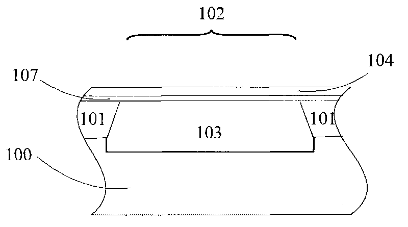
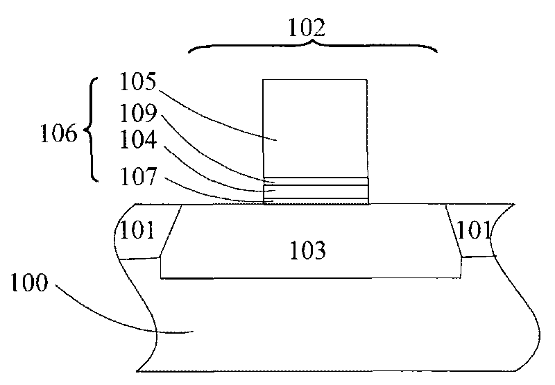
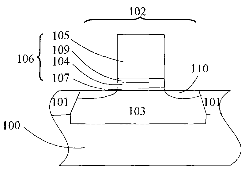
[0037]The present invention uses laser to heat-treat the semiconductor substrate. Due to the characteristics of short laser irradiation time and high intensity, the lattice structure of the native oxide layer naturally oxidized on the semiconductor substrate can be adjusted, and the compactness and uniformity are improved, thereby improving the follow-up process. The quality of the buffer layer and the gate dielectric layer improves the performance of the semiconductor device. In addition, laser heat treatment of the high-K gate dielectric layer can not only repair the defects of the high-K gate dielectric layer, but also reduce the thermal budget of the semiconductor device due to the short time required for laser heat treatment, and improve the local crystallization of the high-K gate dielectric layer. , thereby reducing the generation of leakage current.

[0038] In order to make the above objects, features and advantages of the present invention more comprehensible, specif...


PUM

PropertyMeasurementUnit
thicknessaaaaaaaaaa
thicknessaaaaaaaaaa
thicknessaaaaaaaaaa

Abstract

The invention discloses a method for forming and processing a high-K gate dielectric layer and a method for forming a transistor, wherein the method for forming the high-K gate dielectric layer comprises the following steps: providing a semiconductor substrate; carrying out laser hot treatment on the semiconductor substrate and introducing oxygen or mixed gas of oxygen and nitrogen for forming a buffer layer; and forming the high-K gate dielectric layer on the buffer layer. The invention improves the quality of the subsequent buffer layer and the gate dielectric layer, improves the performance of semiconductor devices, simultaneously reduces the heat budget of the semiconductor devices, improves the local crystallization condition in the high-K gate dielectric layer, and further reduces the generation of the leakage current.

Description

technical field [0001] The invention relates to the field of semiconductor manufacturing, in particular to a method for forming and processing a high-K gate dielectric layer and a method for forming a transistor. Background technique [0002] Since the 1980s, the rapid development of CMOS integrated circuits has promoted the development of the silicon-based microelectronics industry, and the rapid development of CMOS integrated circuits has benefited from the reduction in the size of its basic circuit unit, the field effect transistor. The key factor for the size reduction of field effect transistors is silicon dioxide (SiO2) as the gate dielectric layer. 2 ) decreases in film thickness. The role of silicon dioxide is to isolate the gate and the silicon channel of the semiconductor substrate. As a gate dielectric layer, silicon dioxide has good thermal and electrical stability and good electrical isolation performance. However, as the size of devices continues to shrink, t...

Claims


Application Information

Patent Timeline
Patent Type & Authority Applications(China)
IPC IPC(8): H01L21/28H01L21/31H01L21/336
Inventor 王津洲高大为
Owner SEMICON MFG INT (SHANGHAI) CORP
Why Eureka
Try Eureka