Forming method of CMOS (complementary metal-oxide-semiconductor) transistor

A technology of transistors and semiconductors, applied in semiconductor/solid-state device manufacturing, electrical components, circuits, etc., can solve problems that affect the performance of CMOS transistors, and the performance of CMOS transistors needs to be further improved, so as to reduce thermal budget, improve performance, and achieve good results Effect

Inactive Publication Date: 2015-06-03
SEMICON MFG INT (SHANGHAI) CORP
View PDF3 Cites 7 Cited by
  • Summary
  • Abstract
  • Description
  • Claims
  • Application Information

AI Technical Summary

Problems solved by technology

[0004] There are many defects in the high-K gate dielectric layer formed by the existing process, which will affect the performance of the formed CMOS transistor
Therefore, the performance of the existing CMOS transistors needs to be further improved

Method used


Image

  • Forming method of CMOS (complementary metal-oxide-semiconductor) transistor
  • Forming method of CMOS (complementary metal-oxide-semiconductor) transistor
  • Forming method of CMOS (complementary metal-oxide-semiconductor) transistor

Examples


Embodiment Construction

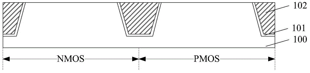
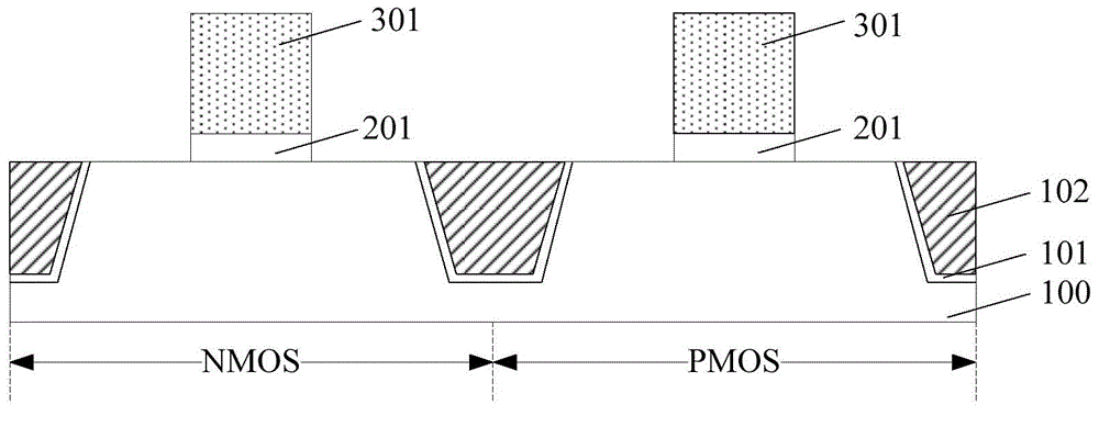
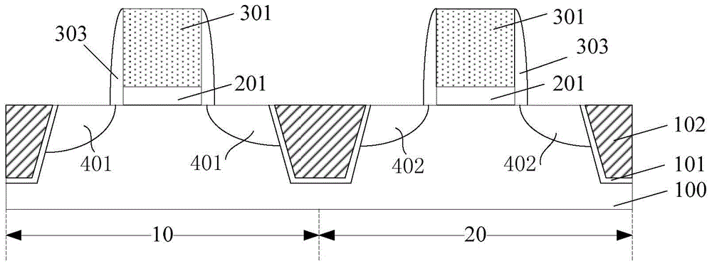
[0027] As mentioned in the background art, in the prior art, there are a large number of defects in the high-K gate dielectric layer formed by the gate-last process, which will greatly affect the performance of the CMOS transistor.

[0028] Research has found that in the gate-front process, the source and drain are formed after the high-K gate dielectric layer and the gate are formed, and the high-K gate dielectric layer is subjected to high temperature at the same time during the annealing process of the source and drain. annealing to reduce the number of defects in the high-K gate dielectric layer. And because in the gate-last process, the high-K gate dielectric layer is formed after the source, drain and dielectric layer, compared with the gate-last process, the high-K gate dielectric layer formed in the gate-last process is subjected to less heat treatment process, This further leads to a large number of defects in the high-K gate dielectric layer formed in the gate-last p...


PUM


Abstract

The invention provides a forming method of a CMOS (complementary metal-oxide-semiconductor) transistor. The forming method comprises the following steps that a semiconductor substrate is provided, the semiconductor substrate comprises an NMOS (N-channel metal oxide semiconductor) region and a PMOS (P-channel metal oxide semiconductor) region, and a shallow groove isolation structure is also formed in the semiconductor substrate; a pseudo grid structure is respectively formed on the surfaces of the NMOS region and the PMOS region; a dielectric layer is respectively formed on the semiconductor substrate and the surface of the shallow groove isolation region; the pseudo grid structure is removed, a first groove is formed in the surface of the NMOS region, and a second groove is formed in the surface of the PMOS region; a high-K grid dielectric material layer is formed, and displacement ions are doped in the high-K grid dielectric material layer, and can overcome defects in the high-K grid dielectric material layer; the high-K grid dielectric material layer is subjected to annealing processing, and the defects in the high-K grid dielectric material layer are further eliminated; a first grid electrode and a second grid electrode are formed. The forming method of the CMOS transistor has the advantage that the quality of the high-K grid dielectric material layer can be improved.

Description

technical field [0001] The invention relates to the technical field of semiconductors, in particular to a method for forming a CMOS transistor. Background technique [0002] With the continuous improvement of the integration level of semiconductor devices and the reduction of technology nodes, the traditional gate dielectric layer continues to become thinner, and the leakage of transistors increases accordingly, causing problems such as waste of power consumption of semiconductor devices. In order to solve the above problems, the prior art provides a solution of replacing the polysilicon gate with a metal gate. Among them, the "gate last" process is a main process for forming high-K metal gate transistors. [0003] The existing method for forming a high-K metal gate transistor using a gate-last process includes: providing a semiconductor substrate on which a dummy gate structure is formed and located on the semiconductor substrate and covering the dummy gate structure An i...

Claims


Application Information

Patent Timeline
Patent Type & Authority Applications(China)
IPC IPC(8): H01L21/8238
CPCH01L21/823857
Inventor 谢欣云
Owner SEMICON MFG INT (SHANGHAI) CORP
Why Eureka
Try Eureka