Double side continuous series welding system for fragment crystal silicon chip and welding method thereof

A technology for crystalline silicon wafers and welding systems, which is applied in semiconductor devices, climate sustainability, sustainable manufacturing/processing, etc., can solve the problems of low welding efficiency, lack of welding equipment, and increased fragmentation rate, etc., and achieve high welding success rate , Improve welding efficiency and reduce the effect of fragmentation rate

Inactive Publication Date: 2009-02-11
天津必利优科技发展有限公司
View PDF0 Cites 10 Cited by
  • Summary
  • Abstract
  • Description
  • Claims
  • Application Information

AI Technical Summary

Problems solved by technology

However, because there is no economical and effective welding equipment, most domestic solar cell module manufacturers use manual welding
The main problems of this welding method are: 1. High requirements for welding personnel, a good welding personnel needs to be trained for a long time, and the training cost is high; 2. The welding

Method used


Image

  • Double side continuous series welding system for fragment crystal silicon chip and welding method thereof
  • Double side continuous series welding system for fragment crystal silicon chip and welding method thereof
  • Double side continuous series welding system for fragment crystal silicon chip and welding method thereof

Examples


Embodiment Construction

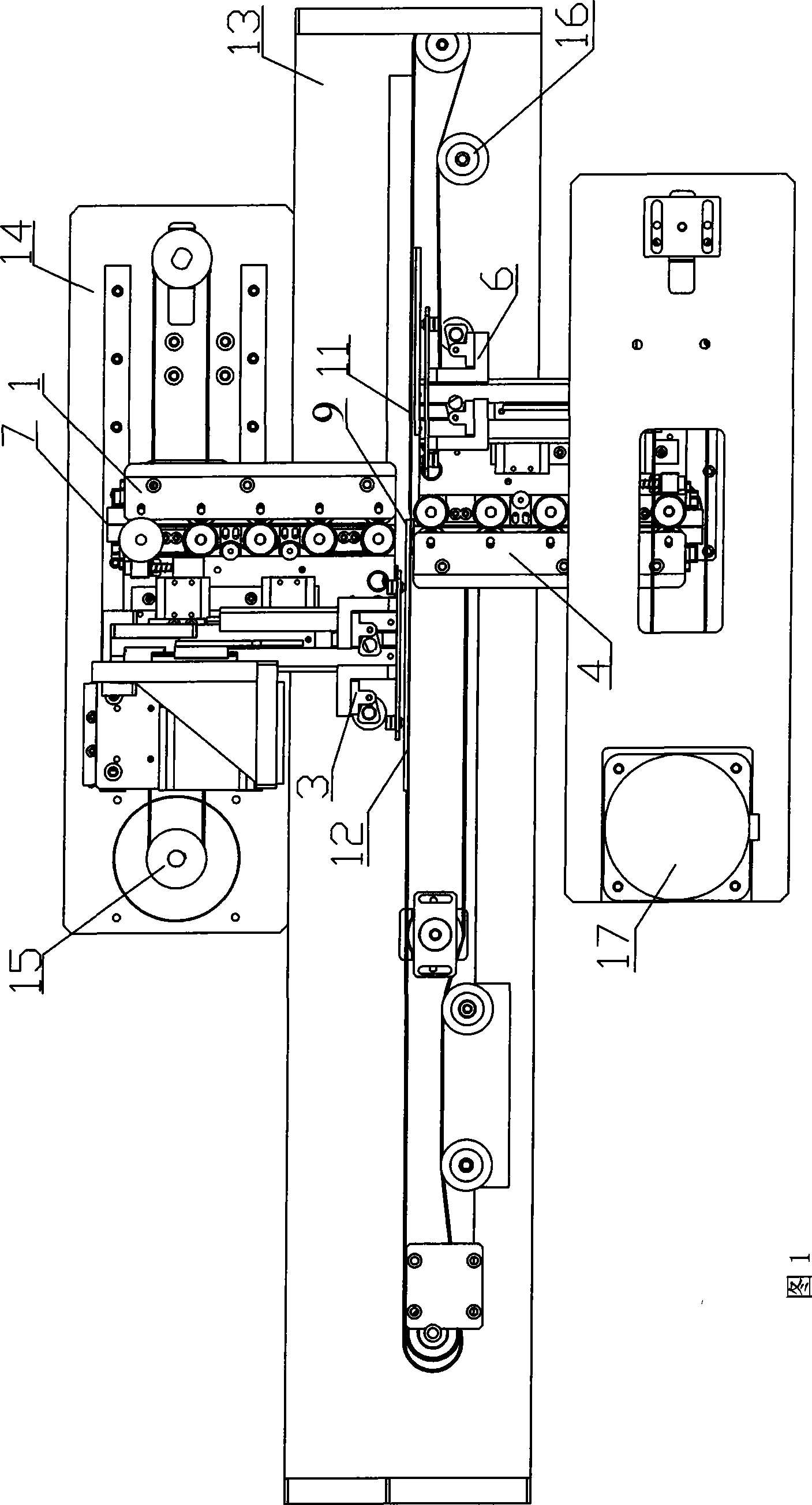
[0060] The double-sided continuous series welding system for fragile crystalline silicon wafers and its welding method of the present invention will be described in detail below with reference to the embodiments and drawings.

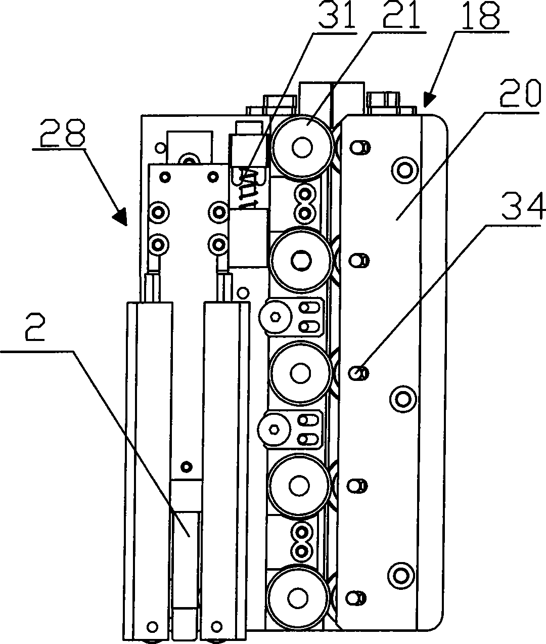
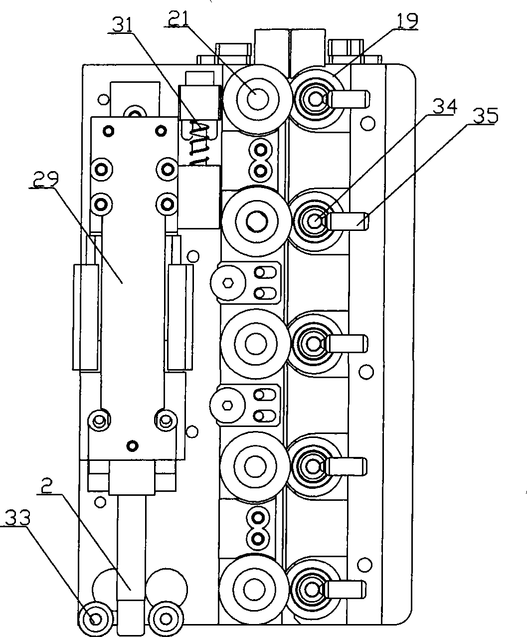
[0061] As shown in Figure 1, the double-sided continuous series welding system for fragile crystalline silicon wafers of the present invention includes a support 13, the upper side of the support 13 is provided with an upper fixing plate 14, and the upper fixing plate 14 is provided with an upper welding assembly 1 that can move in parallel and is used for fixing and conveying the welding strip and welding, and a driving motor 15 that drives the upper welding assembly 1 to move in parallel; the support 13 is located on the upper welding assembly The lower side of 1 is provided with a transmission mechanism 16 that supports and moves the crystalline silicon wafer 11 to be welded, and an upper positioning assembly 3 for positioning the crystalline silicon ...


PUM


Abstract

The invention discloses a double-surface continuous series welding system for a fragile crystal silicon chip and a welding method thereof. An upper fixing plate is arranged on the upper side of a bracket of the system; an upper welded component and a drive motor that drives the upper welded component to conduct parallel movement are arranged on the upper fixing plate; a transport mechanism that supports and transfers the welded crystal silicon chip is arranged on the lower side of the upper welded component on the bracket; an upper locating component for locating an upper welded crystal silicon chip and a solder strip is arranged on the upper side of the transport mechanism; a lower fixing plate is arranged on the lower side of the bracket corresponding to the upper side thereof; a lower welded component symmetrical to the upper fixing plate, and a drive motor that drives the lower welded component to conduct parallel movement are arranged on the lower side of the bracket; and a lower locating component for locating a lower welded crystal silicon chip and a solder strip is arranged on the lower side of the transport mechanism on the bracket. The welding method comprises the following steps: the crystal silicon chips are arranged; the solder strips are installed; each welding component operates; the solder strips are welded on the silicon chips by a welding device; after welding, the previous welded crystal silicon chip is removed and replaced by a new crystal silicon chip for continuous welding. The invention reduces the fragmentation rate and ensures high welding efficiency.

Description

technical field [0001] The invention relates to a welding system for crystalline silicon wafers. In particular, it relates to a double-sided continuous series welding system and welding method for fragile crystal silicon wafers, which can complete single welding and series welding at the same time without secondary welding, improve welding efficiency and reduce fragmentation rate. Background technique [0002] With the gradual popularization of clean energy such as solar energy, the technology of solar cells continues to develop, and the domestic market is also becoming more mature. Solar cell modules are the main products in this market. At present, two important processes in the production of solar cell modules are single welding and series welding of crystalline silicon wafers, and the quality of welding directly affects the efficiency of modules. However, due to the lack of economical and effective welding equipment, most domestic solar cell module manufacturers use ma...

Claims


Application Information

Patent Timeline
IPC IPC(8): H01L31/18H01L21/60
CPCY02P70/50
Inventor 李建平董维来刘贵枝高洪岩孙广合郭素勇
Owner 天津必利优科技发展有限公司
Why Eureka
Try Eureka