Method for digital phase-locked loop and burr elimination

A digital phase-locked loop and order technology, applied in the electronic field, can solve problems such as glitches and achieve the effect of avoiding glitches

Active Publication Date: 2009-02-18
HUAWEI TECH CO LTD
View PDF0 Cites 18 Cited by
  • Summary
  • Abstract
  • Description
  • Claims
  • Application Information

AI Technical Summary

Problems solved by technology

When the DPLL adopts the delay unit of the NAND gate structure, due to the delay of the

Method used


Image

  • Method for digital phase-locked loop and burr elimination
  • Method for digital phase-locked loop and burr elimination
  • Method for digital phase-locked loop and burr elimination

Examples


Embodiment 1

[0044] The embodiment of the present invention provides a digital phase-locked loop, including: MASTER module 601 and SLAVE module 602, and Figure 6 The shown digital phase locked loop is similar, MASTER module 601 includes: master clock processing unit 601a, delay line 601b, phase detector 601c and delay control state machine 601d, SLAVE module 602 includes: ratio logic unit 602a, delay line 602b and output Enable unit 602c. and Figure 6 The difference of the digital phase-locked loop shown is that the SLAVE module 602 provided in this embodiment also includes a flip-flop 602d connected to the delay line 602b, see Figure 7 ,details as follows:

[0045] The flip-flop 602d is used to use the delayed clock signal clk_out to sample the signal of the first delay unit selection terminal msel_0 in the delay line 602b, and output the sampled signal to the second delay unit selection terminal msel in the delay line . The selection terminal msel_0 of the first delay unit is set ...

Embodiment 2

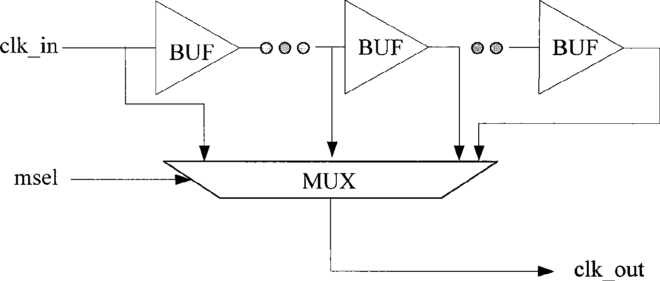
[0051] The embodiment of the present invention also provides a digital phase-locked loop, including: MASTER module 601 and SLAVE module 602, and Figure 6 The same thing as the digital phase-locked loop shown is that the MASTER module 601 includes: a master clock processing unit 601a, a delay line 601b, a phase detector 601c and a delay control state machine 601d, and the SLAVE module 602 includes: a ratio logic unit 602a, a delay line 602b and output enable unit 602c; and Figure 6 The difference of the digital phase-locked loop shown is that the SLAVE module 602 provided in this embodiment also includes a flip-flop 602d and a clock processing unit 602e, and the delay unit in the delay line 602b in this embodiment is composed of an OR gate or a NOR gate . see Figure 10 ,details as follows:

[0052] The flip-flop 602d is used to use the delayed clock signal clk_out to sample the signal of the first delay unit selection terminal msel_0 in the delay line 602b, and output the...

Embodiment 3

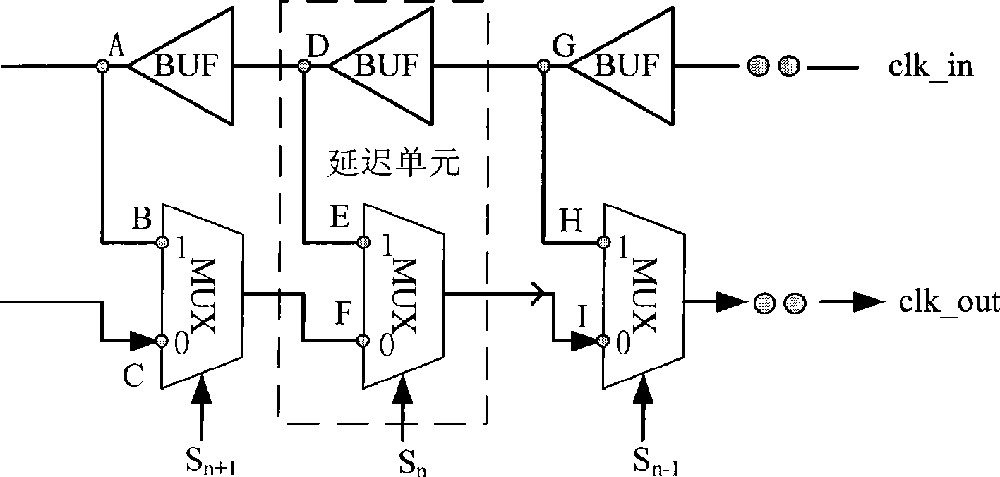
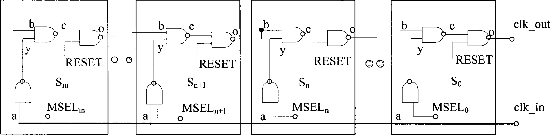
[0062] The embodiment of the present invention also provides a digital phase-locked loop, including: MASTER module 601 and SLAVE module 602, and Figure 10 The difference of the digital phase-locked loop shown is that the SLAVE module 602 provided in this embodiment includes a clock processing unit 602f. In addition to the gate, a second NOT gate is also included, and the delay unit in the delay line 602b in this embodiment is composed of an AND gate or a NAND gate, or is composed of MUX and BUF. see Figure 12 ,details as follows:

[0063] The trigger terminal C of the flip-flop 602d is active at a high level, that is, it is valid after the system clock signal clk is at a low level and the edge of the delayed clock signal clk_out, and other functions are the same as those in Embodiment 2, and the delay line 602b The function is the same as that in Embodiment 2, and will not be repeated here.

[0064] The clock processing unit 602f is configured to perform logic processing ...


PUM


Abstract

The invention discloses a digital phase-locked loop and a method for eliminating spike, belonging to electronic technology field. The digital phase-locked loop includes a trigger and delay lines. the method includes the steps that the trigger receives a delayed clock signal outputted by the delay line from a triggering end, and receives signals of a first delay unit selection end in the delay line from an input end, wherein the selection end of the first delay unit is on a state 1 before triggering the trigger; the trigger samples the signal of the first delay unit selection end using delayed clock signal, and outputs signal after sampling to the selection end of a second delay unit in the delay line, wherein the selection end of the second delay unit is on the state 1 after triggering the trigger. By means of sampling the signal of the selection end of the first delay unit using delayed clock signal by the trigger and using the sampling signal as the signal of the selection end of the second delay unit, the invention avoids the spike caused by jump variation while updating delay module on the clock edge.

Description

technical field [0001] The invention relates to the field of electronic technology, in particular to a digital phase-locked loop and a method for eliminating burrs. Background technique [0002] In many current chips, the information interaction between various signals often requires a certain phase delay relationship between the two. For example, clock signals and data signals, if the clock needs to be able to sample data stably, the rising edge of the clock must be at least one setup time later than the data (register setup time). Affected by process, voltage, and temperature (PVT), the delay requirements between signals will vary, as will the delay of the circuits used to achieve this delay requirement. For example, the most basic unit that constitutes a digital circuit—the NAND gate, whose drive will become higher as the temperature becomes lower or the voltage becomes higher, so its delay will also become smaller. Without compensating for the effect of PVT, the delay ...

Claims


Application Information

Patent Timeline
IPC IPC(8): H03L7/06H03L7/085H03K5/13H03K5/1254
CPCH03L7/0805H03L7/0814H03L7/0818
Inventor 万辰
Owner HUAWEI TECH CO LTD
Why Eureka
Try Eureka