Exposure system and method of manufacturing a semiconductor device

一种曝光系统、光罩的技术,应用在曝光系统领域,能够解决难计测等问题,达到降低生产量、降低制造成本、抑制焦点偏差的效果

Inactive Publication Date: 2009-03-18
PANASONIC CORP
View PDF1 Cites 6 Cited by
  • Summary
  • Abstract
  • Description
  • Claims
  • Application Information

AI Technical Summary

Problems solved by technology

However, since it is a method of measuring the size of the protective layer pattern and obtaining the best focus, it takes time to adjust the best focus
In addition, since it is not the focus measurement of the aerial image, it is difficult to perform the measurement just before exposing each wafer.

Method used


Image

  • Exposure system and method of manufacturing a semiconductor device
  • Exposure system and method of manufacturing a semiconductor device
  • Exposure system and method of manufacturing a semiconductor device

Examples


Embodiment Construction

[0049] Hereinafter, embodiments of the present invention will be described in detail with reference to the drawings. In the following embodiments, the present invention is embodied as a reduced projection exposure apparatus.

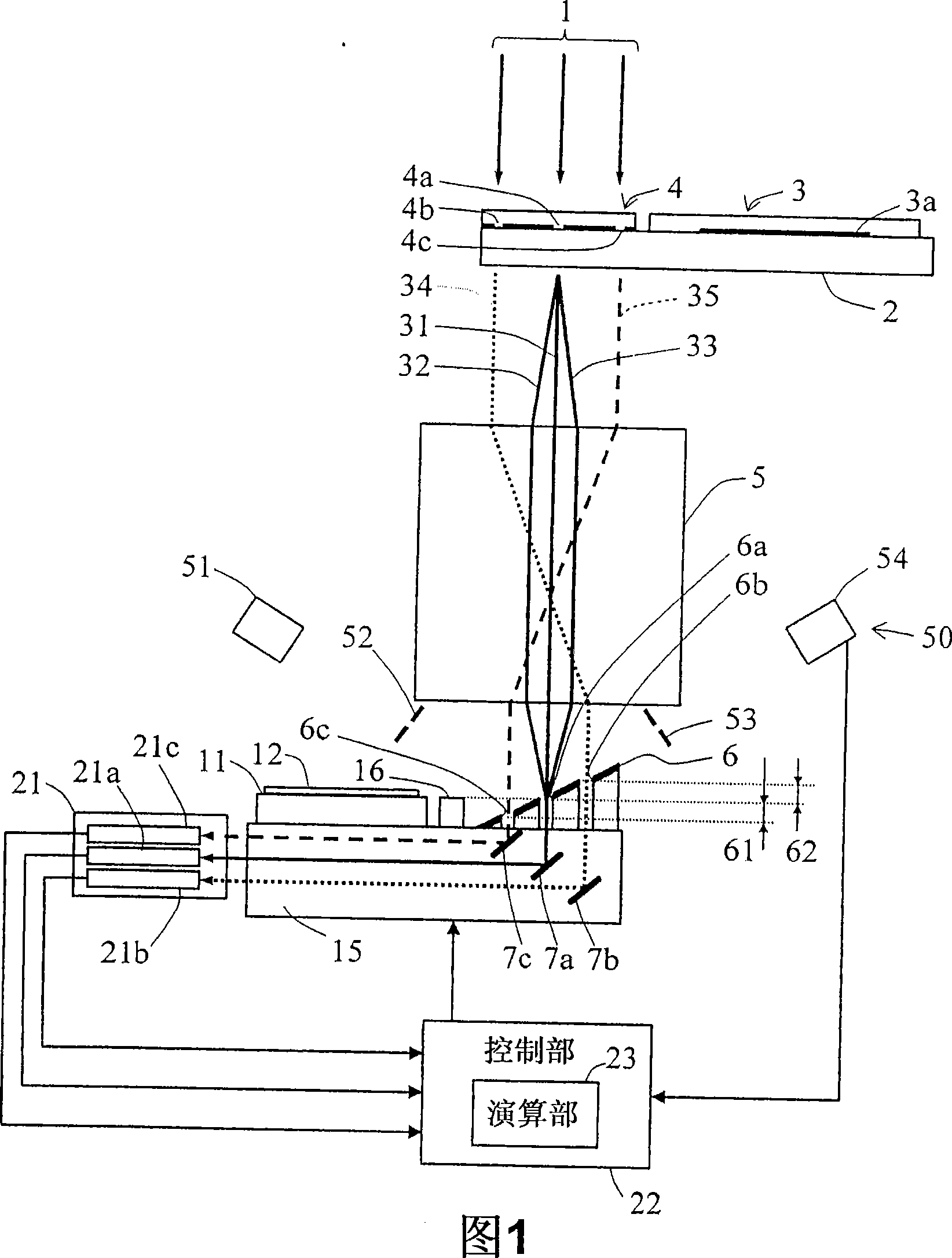
[0050] FIG. 1 is a schematic configuration diagram illustrating the configuration of an exposure apparatus according to an embodiment of the present invention. As shown in FIG. 1, with respect to the exposure apparatus of this embodiment, the exposure light 1 emitted from the exposure light source not shown is irradiated to the mask 3 mounted on the mask stage 2, and passes through the projection lens 5, and makes it appear on the mask 3 The element pattern 3 a formed on the wafer 12 is imaged. The mask stage 2 is arranged between the exposure light source and the projection lens 5 . In addition, on the mask table 2, a spatial image marker body 4 in which a plurality of spatial image markers 4a, 4b, and 4c are arranged is arranged. The mask stage 2 is...


PUM


Abstract

Provided is an exposure system and semiconductor device manufacturing method relating to the present invention, when performing exposure on the wafer in a batch, output is not reduced, generating best focus position. An image of spatial image mark body (4) through a reduction projection lens (5) is projected onto a spatial image projection plate (6) arranged on a wafer stage (15) by irradiating the spatial image mark body (4) arranged on a reticle stage (2) with an exposure light. The spatial image mark body has a plurality of spatial image marks (4a-4c) arranged in a same plane. At projection positions of images of each spatial image mark on the spatial image projection plate (6), spatial image openings (6a-6c) are equipped with differing positions in an optical axis direction of the exposure light. A focus curve with a single exposure can be obtained, without moving the wafer stage (15) in the optical axis direction, by respective measurements of optical intensities of images of each spatial image mark through each opening thereby enabling to calculate the best focus position.

Description

technical field [0001] The present invention relates to an exposure system used in an exposure process for manufacturing semiconductors and the like, and includes a process of measuring a focus setting value of an exposure device for each wafer and adjusting it to the best focus when wafers are exposed in batches. A method of manufacturing a semiconductor device. Background technique [0002] In recent years, in the exposure process of the manufacturing process of semiconductor devices such as semiconductor integrated circuits, exposure apparatuses having a plurality of openings have been used in order to improve the resolution of cell patterns with small dimensions. However, as the number of openings increases, it is necessary to sharply reduce the allowable depth of focus in order to clearly form a cell pattern. Therefore, in the exposure process, it is necessary to set the focus of the exposure device with high precision and perform exposure within an appropriate focal d...

Claims


Application Information

Patent Timeline
Patent Type & Authority Applications(China)
IPC IPC(8): G03F7/20H01L21/027
CPCG03F9/7026G03F9/7034G03F7/70425G03F7/70716
Inventor 西野胜裕吉田孝继
Owner PANASONIC CORP
Why Eureka
Try Eureka