
LED manufacturing method

A manufacturing method and carrier technology, applied in semiconductor/solid-state device manufacturing, electrical components, electrical solid-state devices, etc., can solve the problems of difficult manufacturing, high cost, poor precision, etc., and achieve easy manufacturing, cost reduction, and improved manufacturing accuracy Effect

Active Publication Date: 2009-03-18
SHENZHEN SUNSCREEN CO LTD +1
View PDF0 Cites 4 Cited by
  • Summary
  • Abstract
  • Description
  • Claims
  • Application Information

AI Technical Summary

Problems solved by technology

[0004] The purpose of the embodiments of the present invention is to provide a method for manufacturing LEDs, which aims to solve the problems of poor precision, difficult manufacturing and high cost in the prior art

Method used


Image

  • LED manufacturing method
  • LED manufacturing method
  • LED manufacturing method

Examples


Embodiment Construction

[0038] In order to make the object, technical solution and advantages of the present invention clearer, the present invention will be further described in detail below in conjunction with the accompanying drawings and embodiments. It should be understood that the specific embodiments described here are only used to explain the present invention, not to limit the present invention.

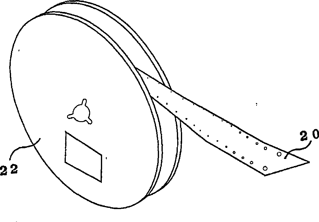
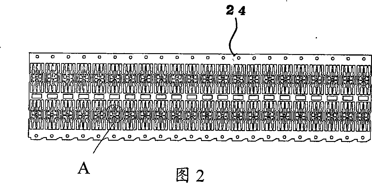
[0039] Such as figure 1 As shown in , the copper metal material sheet 20 in the form of strips is wound in a roll 22 . The present invention uses a tape-and-roll copper metal material blank 20, which is different from the conventional single-piece material blank. The tape-and-roll material blank is suitable for subsequent processes, such as continuous punching, die bonding, wire bonding and dispensing. The procedure can be continuously carried out on the working machine until the end of the reel-type material blank. It is not necessary to remove the completed piece from the working machine after c...


PUM


Abstract

The invention is applied to the production method of an LED, and provides a production method of an LED on a tape type copper metal material sheet. The method comprises the following steps: forming a tape type copper metal material sheet, continuously punching circuits on the tape type copper metal material sheet to form a holder of circuit pattern for placing a diode crystal and electric terminals, plating multi-layer metal on the surface of the holder, continuously spraying metal and molding on the holder to form a protective body for an appointed pattern, providing a groove structure on the upper surface of the protective body, fixing the diode crystal on a holder which is located on the bottom of the groove structure of the protective body, and connecting the electrode terminals of the diode crystal and the terminal contacts of the holder through metal wires. The invention can improve the problem of LED production precision, makes production accurate and easy, and effectively reduces cost.

Description

technical field [0001] The invention belongs to a method for manufacturing an LED, in particular to a method for manufacturing an LED located on a roll-type copper metal material sheet. Background technique [0002] The selection of LED packaging methods, materials and packaging equipment is mainly determined by factors such as the function, electrical or photoelectric characteristics, precision and unit price of the LED chip. After decades of development, the LED industry has gone through the development process of bracket LED (Lead LED), ordinary chip LED (Chip SMD LED), power LED (Power LED) and high power LED (High Power LED). [0003] When manufacturing a single-chip LED carrier, porcelain is used as the material for the carrier, and it is not easy to form circuits on the surface of the carrier, that is, it is not easy to form a circuit pattern on the carrier, which is difficult to manufacture, and the precision is poor and the cost is high. If a metal (such as copper)...

Claims


Application Information

Patent Timeline
Patent Type & Authority Applications(China)
IPC IPC(8): H01L33/00H01L21/48H01L21/60H01L33/48
CPCH01L2924/01322H01L2224/45124H01L2924/01078H01L2924/3011H01L2924/01079H01L2224/48091H01L2224/45147H01L2224/45144H01L2924/01047
Inventor 宋文洲
Owner SHENZHEN SUNSCREEN CO LTD
Learn More