
Built-in self-testing circuit and clock switching circuit of programmable memory

A built-in self-test circuit and built-in self-test technology, applied in static memory, instruments, etc., can solve the problems of increased production cost, difficult test work, large chip area, etc., to reduce the area, increase the area, and reduce the chip size. area effect

Inactive Publication Date: 2009-04-01
FARADAY TECH CORP
View PDF0 Cites 20 Cited by
  • Summary
  • Abstract
  • Description
  • Claims
  • Application Information

AI Technical Summary

Problems solved by technology

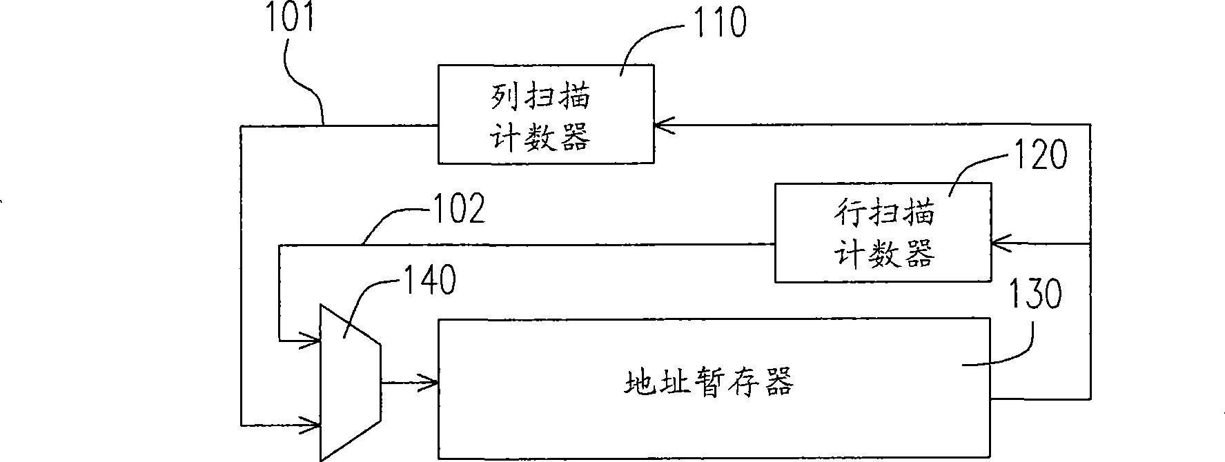
Once the size of the memory is very large, its relative number of address bits will also increase, causing the row scan counter 120 and the column scan counter 110 to occupy a large chip area, resulting in an increase in production costs
[0005] Another difficulty of the known built-in self-test circuit of the memory is that the clock frequency provided by the current automatic test equipment (auto test equipment, ATE) is much lower than the clock frequency of the built-in self-test circuit of the memory, so in the self-test mode There will be a clock hazard due to clock switching between the test with the external automatic test equipment. This clock hazard will cause unpredictable phenomena in subsequent test operations, resulting in misoperation or non-operation, resulting in test work Difficulties

Method used


Image

  • Built-in self-testing circuit and clock switching circuit of programmable memory
  • Built-in self-testing circuit and clock switching circuit of programmable memory
  • Built-in self-testing circuit and clock switching circuit of programmable memory

Examples


Embodiment Construction

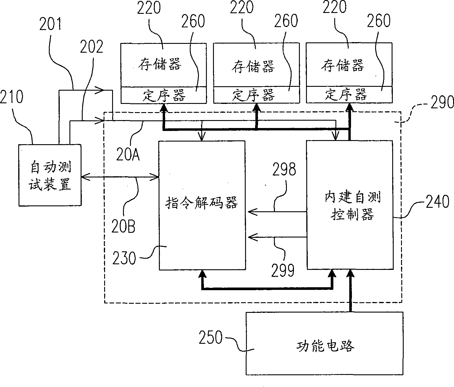
[0076] Figure 2A It is an embodiment of the memory built-in self-test circuit of the present invention, which includes a memory built-in self-test circuit 290, a memory under test 220, a sequencer (sequencer) 260 to which the memory under test 220 belongs, and an external automatic test device 210 and a functional circuit 250 . Each tested memory 220 and its corresponding sequence generator 260 are respectively coupled with the memory built-in self-test circuit 290, the memory built-in self-test circuit 290 is coupled with the automatic test device 210, and the function circuit 250 is also connected with the memory built-in self-test circuit 290. Built-in self-test circuit 290 is coupled.

[0077] Please refer to Figure 2A As shown, the memory built-in self-test circuit 290 includes a command decoder 230 and a built-in self-test controller 240 coupled to each other. The built-in self-test controller 240 and the instruction decoder 230 receive the control signal 20A, where...


PUM


Abstract

The invention provides a programmable memory build-in self-test circuit and a clock switching circuit. Through an instruction decoder and a built-in test controller, more self-test functions can be set by users, abundant circuits in the traditional technology are simplified, and the area of a chip is lowered to reduce the cost. Control circuits around the memory are also provided. Less area is occupied. The position of the memory can be tested more flexibly. The clock switching circuit is also provided. The chip can be correctly tested at clocks of different speeds. The testability and the analyzability of the memory in the chip can be improved. And the error covering rate is improved.

Description

technical field [0001] The present invention relates to a built-in self-test circuit, and in particular to a memory built-in self-test circuit and its address counter and clock switching circuit. Background technique [0002] As semiconductors enter the very deep sub-micro (VDSM) process, chip design becomes more complex and sophisticated, and most products require memory to handle complex and diverse calculations. However, because memory testing requires a large number of test patterns (Test Pattern), and many input / output ports are not easy to connect to the outside of the chip, so a memory built-in self test circuit (memory built-in self test, MBIST) ) was proposed, and this testing technology is to use the circuit built in the memory chip to perform read and write tests on the internal memory circuit during a specific period. To determine whether the memory chip is good or bad. [0003] In the traditional memory built-in self-test circuit, several algorithms are usuall...

Claims


Application Information

Patent Timeline
IPC IPC(8): G11C29/20
Inventor 张永嘉林重甫
Owner FARADAY TECH CORP
Learn More