Multi-chip 3D stacking and packaging structure

A packaging structure, multi-chip technology, applied in electrical components, electrical solid devices, circuits, etc., can solve problems such as poor signal transmission performance, large space for multi-chip packaging structures, and high packaging manufacturing costs.

Inactive Publication Date: 2009-04-08
HUAYA MICROELECTRONICS (SHANGHAI) INC
View PDF0 Cites 12 Cited by
  • Summary
  • Abstract
  • Description
  • Claims
  • Application Information

AI Technical Summary

Problems solved by technology

[0003] The technical problem to be solved by the present invention is to provide a multi-chip 3D stacked packaging structure to solve the technical problems of the current multi-chip packaging structure with large space, poor signal transmission performance and high packaging and manufacturing costs

Method used


Image

  • Multi-chip 3D stacking and packaging structure
  • Multi-chip 3D stacking and packaging structure
  • Multi-chip 3D stacking and packaging structure

Examples


Embodiment Construction

[0019] The following is based on Figure 1 to Figure 6 , give a preferred embodiment of the present invention, and give a detailed description, so that the functions and characteristics of the present invention can be better understood.

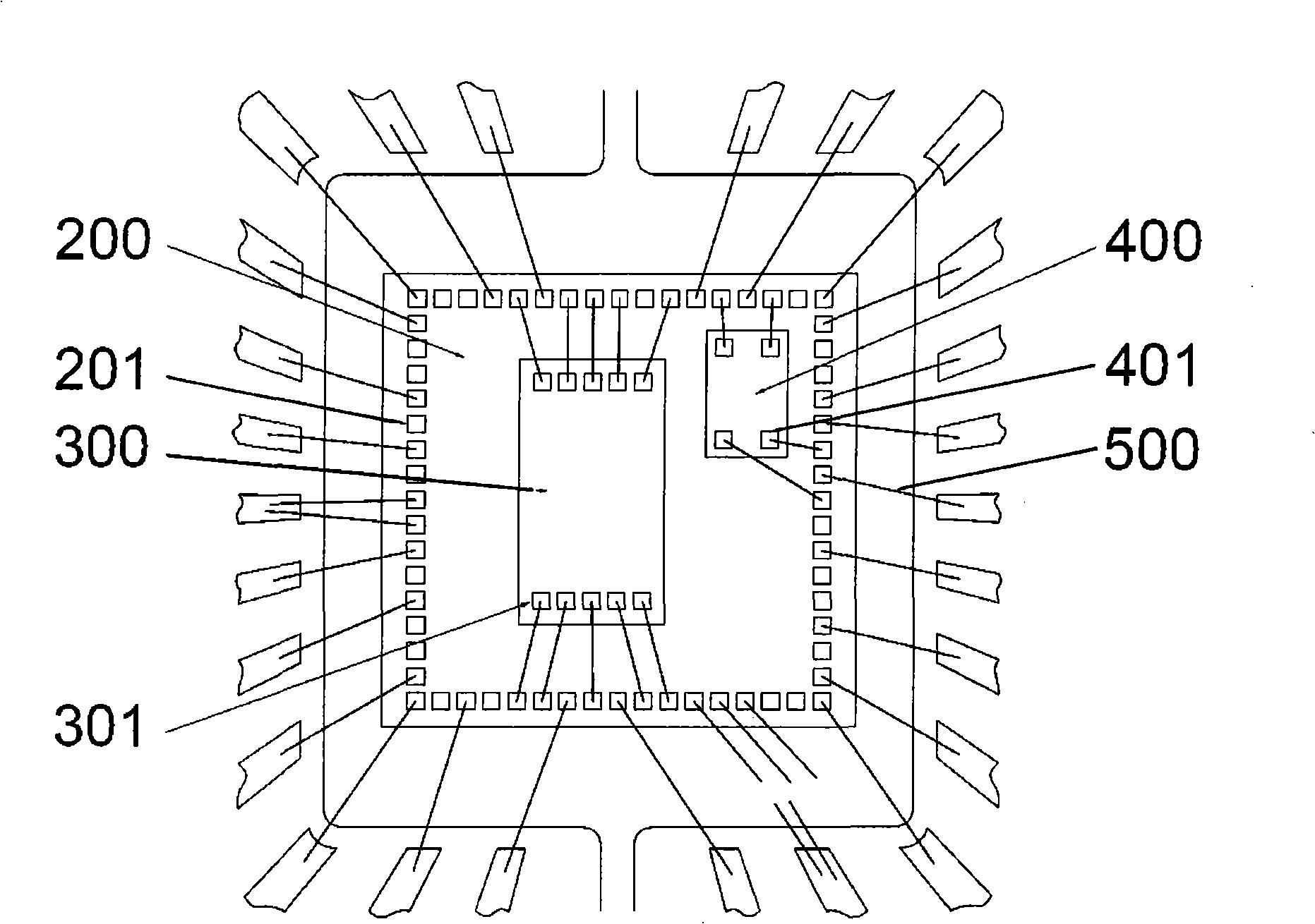
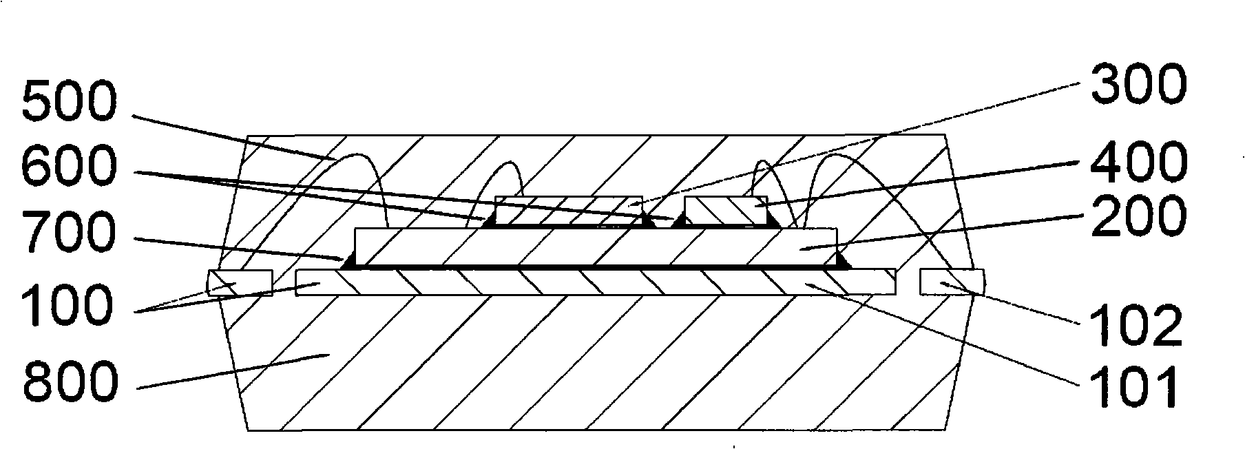
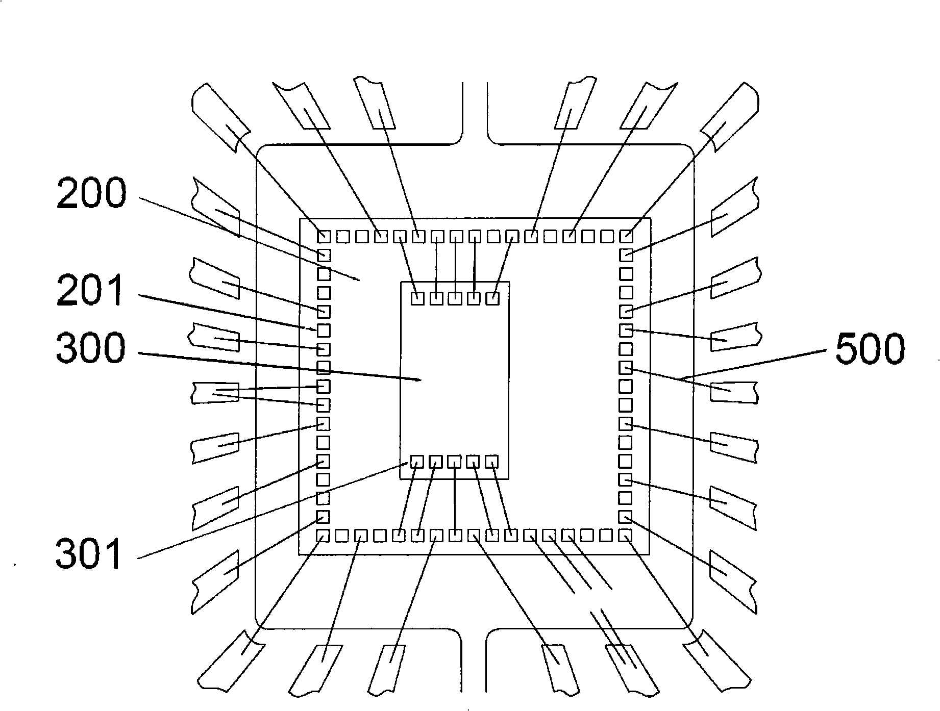
[0020] figure 1 What is shown is a schematic top view of the three-chip 3D stacked package structure of the present invention. A circle of welding pads 201 is formed on the periphery of the circuit surface of the main chip 200. The welding pads 201 can be as follows: figure 1 The single-row distribution shown can also be a double-row distribution (not shown). A row of bonding pads 301 are respectively provided on the upper and lower sides of the auxiliary chip 300 . A plurality of bonding pads 401 are disposed on the periphery of the auxiliary chip 400 . The arrangement of the bonding pads 201 of the main chip 200 is matched with the arrangement of the bonding pads 301 of the auxiliary chip 300 and the bonding pads 401 of the auxiliary chi...


PUM


Abstract

The invention relates to a multi-chip 3D stacked packaging structure. The structure comprises a main chip and at least one auxiliary chip. The main chip and the auxiliary chip are respectively provided with a circuit surface and a back surface facing the circuit surface; the auxiliary chip is stacked on the main chip; a main bonding pad is arranged on the circuit surface of the main chip, and an auxiliary bonding pad is arranged on the circuit surface of the auxiliary chip; the auxiliary bonding pad is connected with the main bonding pad by a metal wire. By using the multi-chip 3D stacked packaging structure, the main chip for video processing is designed to connect a plurality of auxiliary chips completely by internal leads in a package, and the functional integration of three chips in a dual in-line package is finished. High formation degree of the chip reduces the area of a circuit board, lowers the production cost of manufacturers, reduces the signal transmission delay and improves the system performance simultaneously. And the system board and the module have the advantages of small packaging size and light weight.

Description

technical field [0001] The invention relates to an integrated circuit package structure, in particular to a dual in-line package multi-chip 3D stacked integrated circuit package structure, which can be used to package multiple semiconductor chips. Background technique [0002] In the past, the video processing chips and flash and DRAM chips necessary for the system were packaged separately into independent ICs, and after the packaging was completed, the manufacturers put them on the board to form the system. This system structure wastes space in the circuit board design, and there are problems such as signal delay in signal transmission, and the cost is relatively high. However, Flash and DRAM multi-chip stack packages are generally high-end BGA or QFP. These two packages must use double-sided panels when designing circuit boards, and the overall system cost is relatively high. Contents of the invention [0003] The technical problem to be solved by the present invention ...

Claims


Application Information

Patent Timeline
Patent Type & Authority Applications(China)
IPC IPC(8): H01L25/00H01L25/18H01L23/488
CPCH01L2224/32245H01L2924/19107H01L2224/73265H01L2224/48257H01L2224/48247H01L2924/01047H01L2224/32145H01L2224/45144H01L2224/48145H01L2224/4911H01L2224/45147H01L2224/49171H01L2224/45139H01L2924/00014H01L2924/00H01L2924/00012H01L2224/45015H01L2924/207
Inventor 李云芳
Owner HUAYA MICROELECTRONICS (SHANGHAI) INC
Why Eureka
Try Eureka