Method for manufacturing liquid crystal panel and method for cutting substrate

A manufacturing method and liquid crystal panel technology, applied in the direction of manufacturing tools, instruments, laser welding equipment, etc., can solve problems such as coolant residue, and achieve the effects of improving yield, improving quality, and high-quality substrates

Inactive Publication Date: 2009-04-15
INNOCOM TECH SHENZHEN +1
View PDF0 Cites 14 Cited by
  • Summary
  • Abstract
  • Description
  • Claims
  • Application Information

AI Technical Summary

Problems solved by technology

[0017] In order to solve the problem that the liquid crystal panel manufacturing method in the prior art is prone to coolant residue, it is necessary to provide a liquid crystal panel manufacturing method that reduces the coolant residue and improves product quality

Method used


Image

  • Method for manufacturing liquid crystal panel and method for cutting substrate
  • Method for manufacturing liquid crystal panel and method for cutting substrate
  • Method for manufacturing liquid crystal panel and method for cutting substrate

Examples


Embodiment Construction

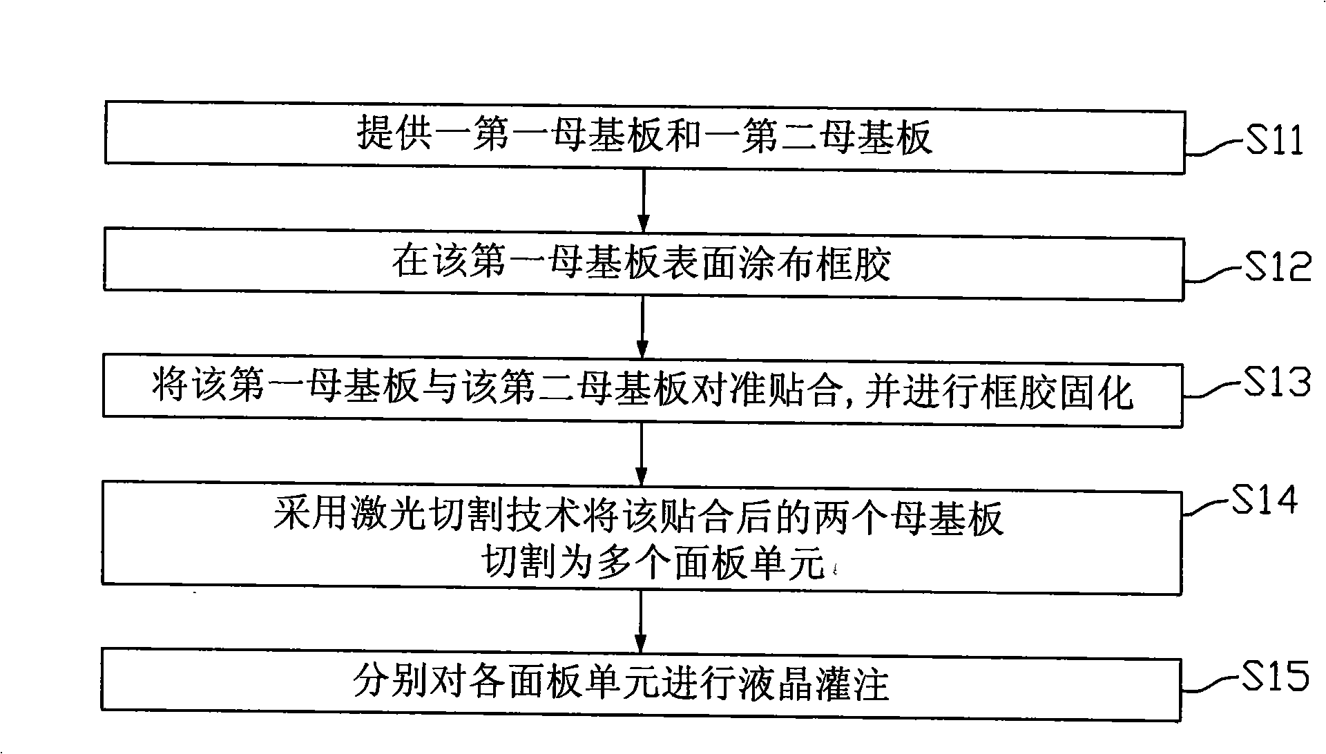
[0035] see figure 1 , is a flow chart of the first embodiment of the liquid crystal panel manufacturing method of the present invention. The manufacturing method of the liquid crystal panel includes the following steps: providing a first mother substrate and a second mother substrate; coating a sealant on the surface of the first mother substrate; aligning and laminating the first mother substrate and the second mother substrate , and curing the frame glue; cutting the laminated first and second mother substrates into multiple panel units by using laser cutting technology; performing liquid crystal perfusion on each panel unit respectively. Among them, the details of each step are as follows:

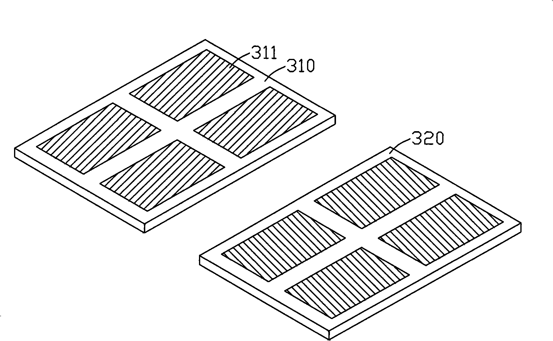
[0036] Step S11, providing a first motherboard 310 and a second motherboard 320;

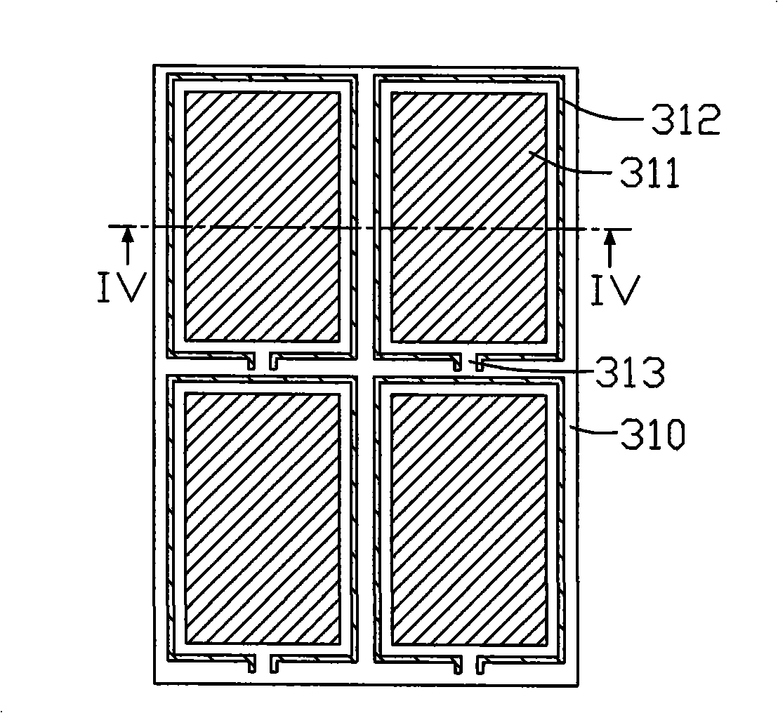
[0037] Please also refer to figure 2 , is a schematic perspective view of the first mother substrate 310 and the second mother substrate 320 . The step S11 is specifically as follows: Firstly, a firs...


PUM


Abstract

The invention provides a method for manufacturing a liquid crystal panel. The method comprises: two mother boards are provided; the two mother boards are jointed with each other; the two jointed mother boards are irradiated by laser; and the area irradiated by laser is cooled by a refrigerant which contains supercritical fluid. The invention also provides a method for cutting a base plate.

Description

technical field [0001] The invention relates to a liquid crystal panel manufacturing method and a substrate cutting method. Background technique [0002] Liquid crystal display devices are widely used in modern information equipment, such as monitors, televisions, mobile phones, and digital products, due to their advantages of light weight, low power consumption, low radiation, and easy portability. [0003] A liquid crystal display device usually includes a liquid crystal panel and a backlight module stacked, wherein the liquid crystal panel includes a thin film transistor array substrate and a color filter substrate oppositely arranged, and a sandwiched between the two substrates liquid crystal layer. In order to increase production and reduce costs, in the production process, a plurality of thin film transistor array units are usually fabricated on one mother substrate, and a plurality of color filter units are fabricated on another mother substrate; and the above two mo...

Claims


Application Information

Patent Timeline
Patent Type & Authority Applications(China)
IPC IPC(8): G02F1/1333B23K26/38B23K26/00B23K26/70
Inventor 谷祖贤吴佳怡萧坤星
Owner INNOCOM TECH SHENZHEN
Why Eureka
Try Eureka