Check patentability & draft patents in minutes with Patsnap Eureka AI!

Method for forming polysilicon film

一种多晶硅、非晶硅膜的技术,应用在气态化学镀覆、涂层、电气元件等方向,能够解决很难满足微细加工等问题

Active Publication Date: 2009-04-15
TOKYO ELECTRON LTD
View PDF2 Cites 4 Cited by
  • Summary
  • Abstract
  • Description
  • Claims
  • Application Information

AI Technical Summary

Problems solved by technology

However, the phosphorus-doped polysilicon film formed by the above-mentioned technology has a lower limit of crystal grain size of about 300nm, which is difficult to meet the requirements of microfabrication.

Method used


Image

  • Method for forming polysilicon film
  • Method for forming polysilicon film
  • Method for forming polysilicon film

Examples


Embodiment Construction

[0022] Hereinafter, embodiments of the present invention will be described with reference to the drawings. However, in the following description, components having substantially the same function and structure are denoted by the same reference numerals, and descriptions are repeated only when necessary.

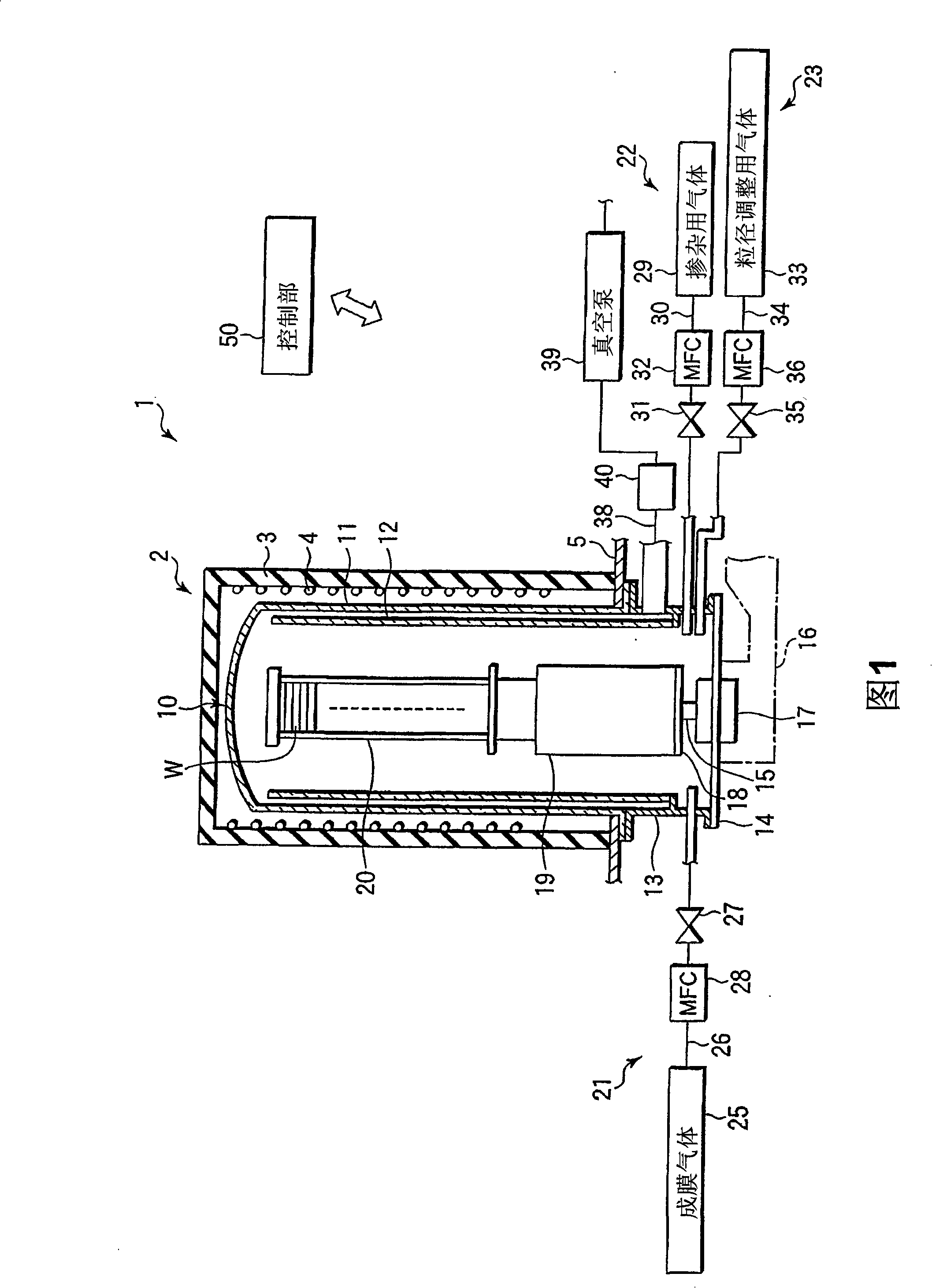
[0023] FIG. 1 is a longitudinal sectional view of an example of a film forming apparatus for carrying out a film forming method according to an embodiment of the present invention. The film forming apparatus 1 has a heating furnace 2 including: a cylindrical heat insulator 3 having a top; and a heater 4 provided on the inner peripheral surface of the heat insulator 3 . The heating furnace 2 is arranged on a base 5 .

[0024] Inserted in the heating furnace 2 is a reaction tube 10 as a reaction vessel. The reaction tube 10 is formed to have an outer tube 11 made of, for example, quartz and whose upper end is closed, and an inner tube made of, for example, quartz which is conc...


PUM

PropertyMeasurementUnit
particle diameteraaaaaaaaaa

Abstract

The present invention relates to a method for forming polycrystalline silicon film, which is used to form polycrystalline silicon film doped with phosphorus or boron. The method is characterized by including the following processes: configuring the substrate to be processed in the reaction container; heating the substrate to be processed under pressure reduction situation, at the same time introducing a silicon film-forming gas, a gas doped with phosphorus or boron, and a particle diameter modulation gas which contains component preventing the column crystallization of the polycrystalline silicon and promoting the micro crystallization of the polycrystalline silicon; and accumulating a silicon film doped with phosphorus or boron on the substrate to be processed.

Description

technical field [0001] The present invention relates to a method for forming a polysilicon film on a substrate to be processed such as a semiconductor wafer, and in particular to a technique used in semiconductor processing. Here, semiconductor processing refers to forming semiconductor layers, insulating layers, conductive layers, etc. Various processes performed to manufacture structures including semiconductor devices, wiring connected to the semiconductor devices, electrodes, etc., on the object to be processed. Background technique [0002] A semiconductor device is formed by stacking various thin films, and a polysilicon film doped with phosphorus (P) and boron (B) is used as such a thin film. Such a doped polysilicon film is used as a resistor element, a gate electrode, a wiring, and the like. [0003] When forming such doped polysilicon, since it is excellent in controllability and does not cause damage to the substrate such as ion entry, decompression CVD (Chemica...

Claims


Application Information

Patent Timeline
Patent Type & Authority Applications(China)
IPC IPC(8): H01L21/205
CPCH01L21/02573H01L21/28035H01L21/02667C23C16/24H01L21/0262C23C16/56H01L21/0257H01L21/0256H01L21/02579H01L21/02532H01L21/02595
Inventor 冈田充弘宫原孝广西村俊治
Owner TOKYO ELECTRON LTD
Features
  • R&D
  • Intellectual Property
  • Life Sciences
  • Materials
  • Tech Scout
  • Unparalleled Data Quality
  • Higher Quality Content
  • 60% Fewer Hallucinations
Learn More