Developing method and developer coating apparatus

A technology of coating device and developer, which can be used in electrical components, semiconductor/solid-state device manufacturing, circuits, etc., and can solve problems such as the reduction of developer

Inactive Publication Date: 2009-05-06
TOKYO ELECTRON LTD
View PDF0 Cites 4 Cited by
  • Summary
  • Abstract
  • Description
  • Claims
  • Application Information

AI Technical Summary

Problems solved by technology

[0008] After the development reaction is completed, when pure water is supplied to the semiconductor wafer, the pH of the developer on the semiconductor wafer drops sharply, so the dissolved product solid is precipitated and attached to the developed pattern, which may cause defects

Method used


Image

  • Developing method and developer coating apparatus
  • Developing method and developer coating apparatus
  • Developing method and developer coating apparatus

Examples


Embodiment Construction

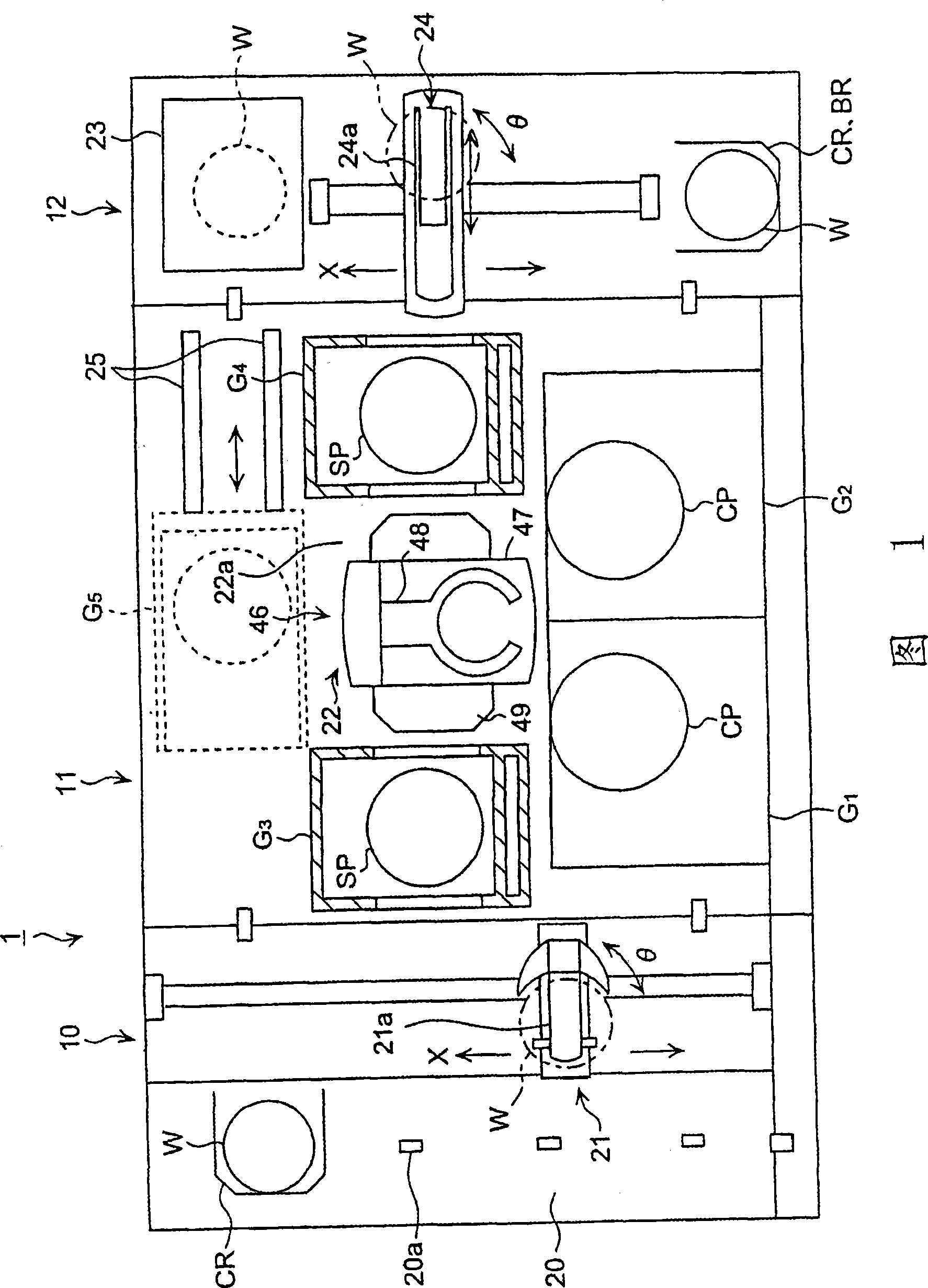
[0042] Hereinafter, embodiments of the present invention will be described in detail with reference to the accompanying drawings. Here, a description will be given of a development treatment method using a resist application and development treatment system that continuously performs the application of the resist to the semiconductor wafer (wafer) to the development treatment.

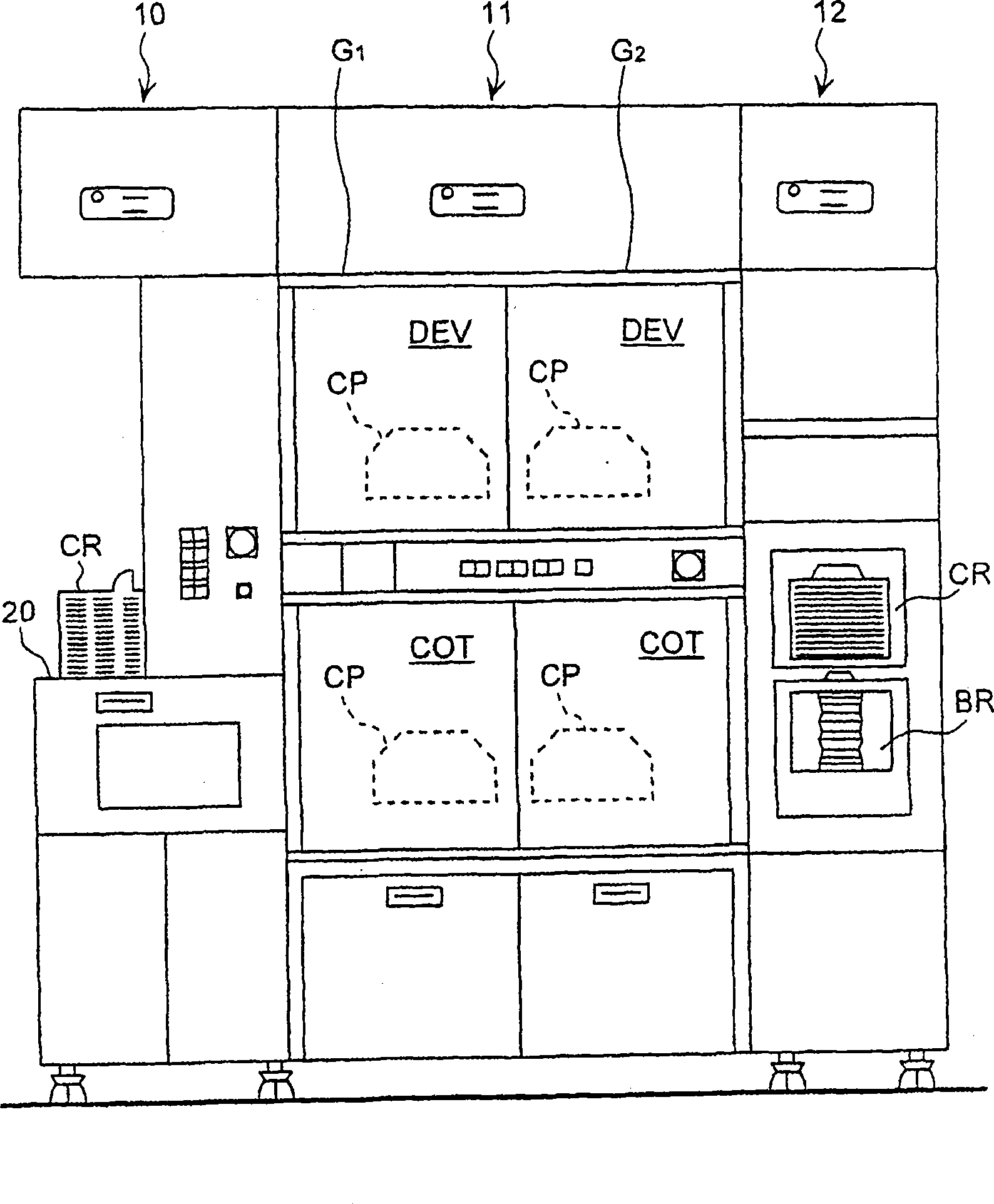
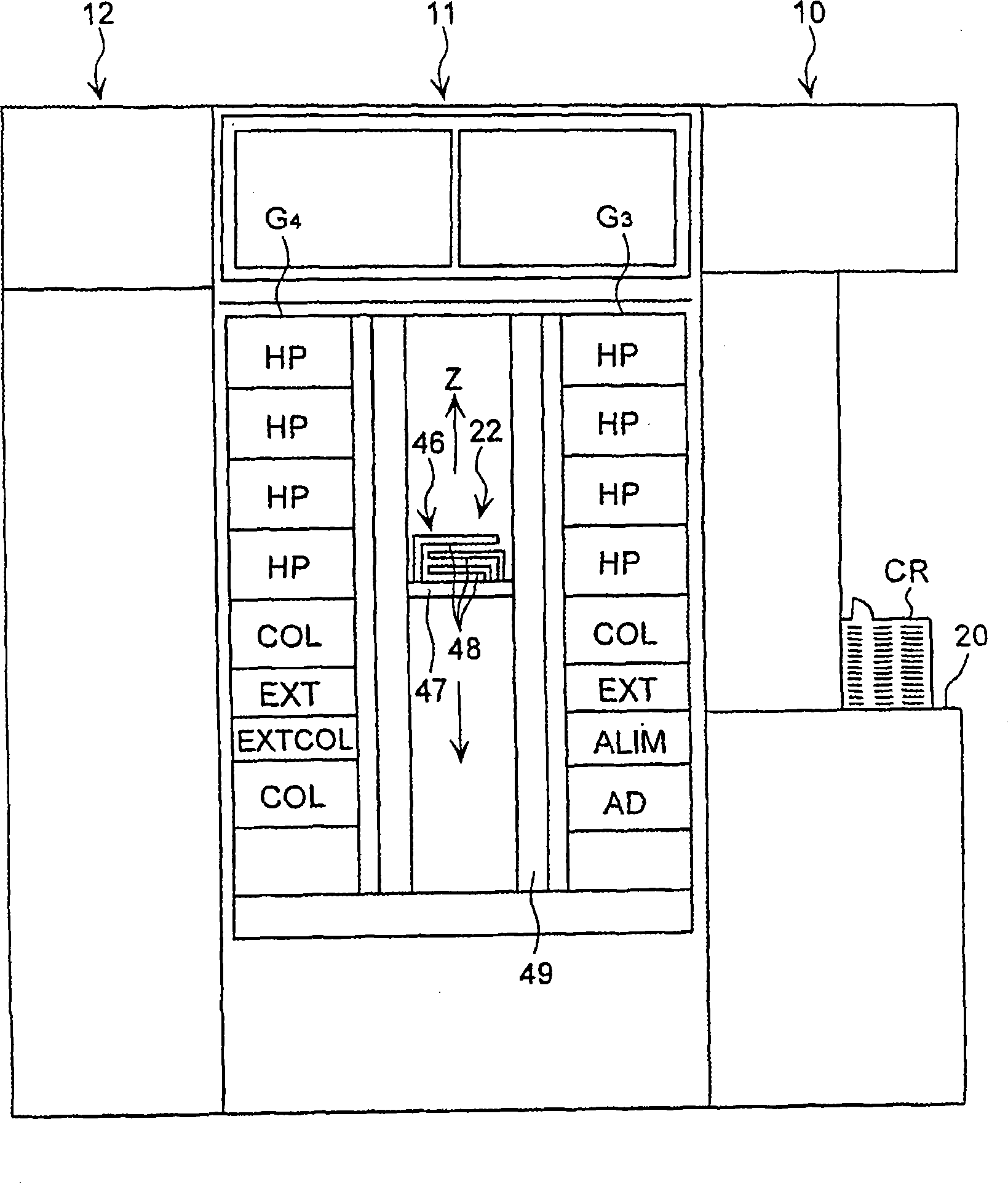
[0043] FIG. 1 is a schematic plan view showing a resist coating and developing processing system, figure 2 is its front view, image 3 is its rear view. This resist coating and developing processing system 1 has a box table 10 as a conveying table, a processing table 11 having a plurality of processing units, and a processing table 11 provided adjacent to the processing table 11 for transferring wafers W between exposure devices not shown the interface part 12.

[0044] The box table 10 carries out the transportation from another system to the present resist coating and developing processing system ...


PUM


Abstract

A developing liquid coating device is disclosed, including: a developing liquid nozzle; a first delivering device that delivers the developing liquid with a predetermined concentration; a second delivering device that delivers pure water and the developing liquid having the concentration different than that of the developing liquid delivered by the first delivering device; the developing liquid nozzle includes: a first liquid storing chamber for storing the developing liquid delivered from the first delivering device; a second liquid storing chamber for storing the pure water and the developing liquid delivered from the second delivering device; a liquid blending chamber that has a developing liquid ejecting hole and that is communicated with the first and the second liquid storing chambers; a first path that communicates the first liquid storing chamber with the liquid blending chamber; a second path that communicates the second liquid storing chamber with the liquid blending chamber; the developing liquid or the pure water or the developing liquid having different concentration is ejected from the developing liquid ejecting hole, the developing liquid stored in the first liquid storing chamber and the pure water or the developing liquid having different concentration both stored in the second liquid storing chamber are blended in the liquid blending chamber in order to prepare the developing liquid having the prescribed concentration which is ejected from the developing liquid ejecting hole.

Description

[0001] This application is a divisional application of a Chinese patent application with the patent application number 02143756.4, the application date is August 28, 2002, and the invention title is "Development Treatment Method and Developer Solution Coating Device". technical field [0002] The present invention relates to a development treatment method and a developer solution coating apparatus for subjecting a substrate such as a semiconductor wafer to an exposure treatment to a development treatment. Background technique [0003] In the manufacture of semiconductor devices, a so-called photolithography technique is used to form a predetermined circuit pattern on the surface of a semiconductor wafer. In this photolithography step, for example, a photoresist liquid is applied on a cleaned semiconductor wafer to form a resist film, and the resist film is exposed to a predetermined pattern and developed. [0004] In such a development treatment step, the semiconductor wafer...

Claims


Application Information

Patent Timeline
IPC IPC(8): G03F7/30H01L21/00
Inventor 吉原孝介田中启一山本太郎京田秀治竹口博史大河内厚
Owner TOKYO ELECTRON LTD
Why Eureka
Try Eureka