Layout structure of non-volatile memory

Inactive Publication Date: 2008-01-17
MACRONIX INT CO LTD
View PDF10 Cites 6 Cited by
  • Summary
  • Abstract
  • Description
  • Claims
  • Application Information

AI Technical Summary

Benefits of technology

[0006]In view of the foregoing, this invention provides a layout structure of non-volatile memory that can improve the CD uniformity.
[0007]This invention also provides a layout structure of non-volatile memory that can improve the CD uniformity as well as improve the lithography process window.
[0012]Since dummy word line patterns are added at two sides of the active area, i.e., beside the word line patterns, the CD difference between the edge portions and the central portion of the memory array can be decreased. Moreover, because the dummy word lines are disposed on the isolation structure but not on the active area, the size of the active area is not increased, and no transistor is formed from the dummy word lines to cause leakage or performance degradation to the device.

Problems solved by technology

For example, the critical dimension (CD) at edges of a memory array is easily different from that at the center of the same due to the lithographic optics, so that a malfunction like leakage or short circuit is often caused lowering the yield and reliability of the memory device.

Method used


Image

  • Layout structure of non-volatile memory
  • Layout structure of non-volatile memory
  • Layout structure of non-volatile memory

Examples


Embodiment Construction

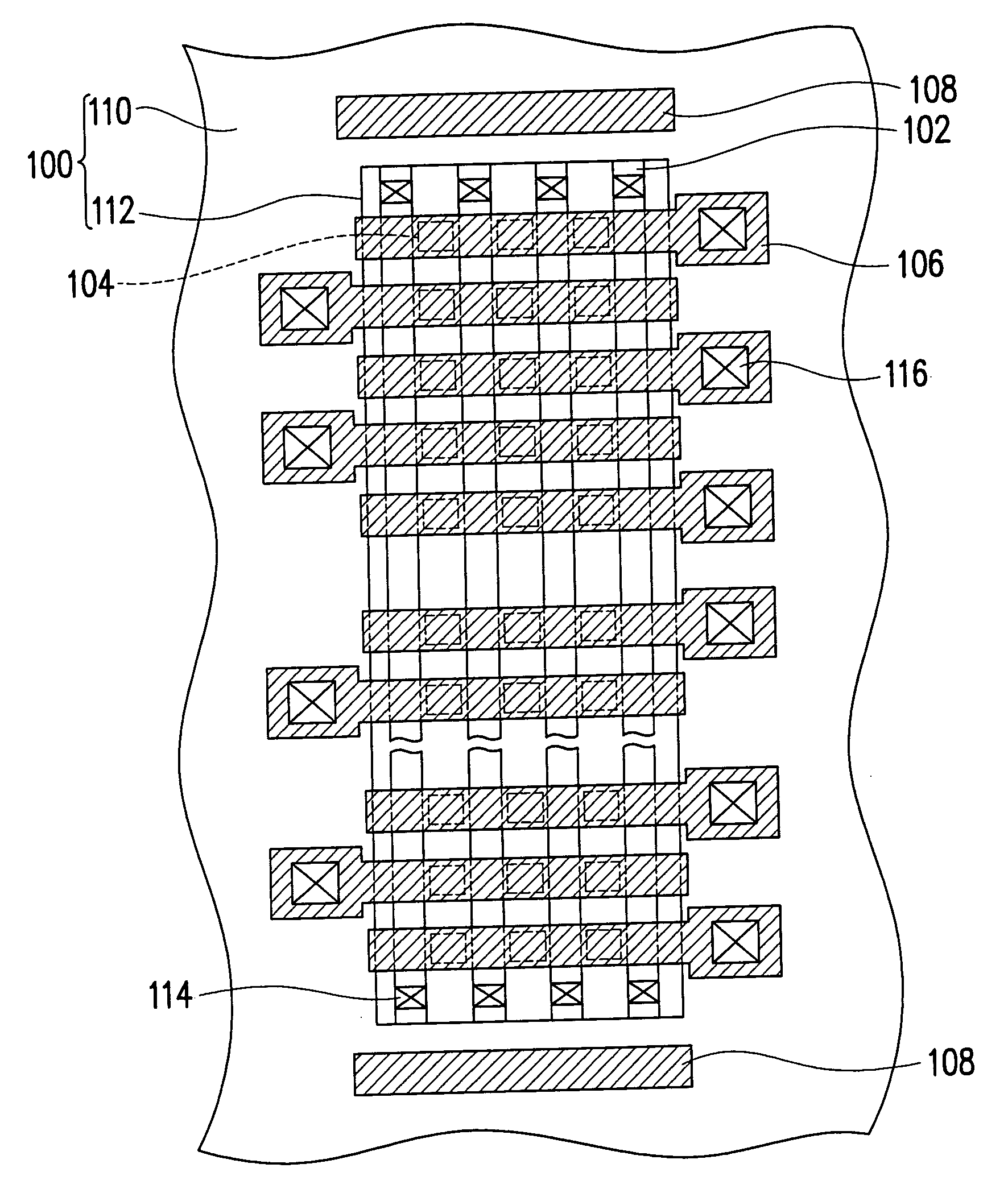
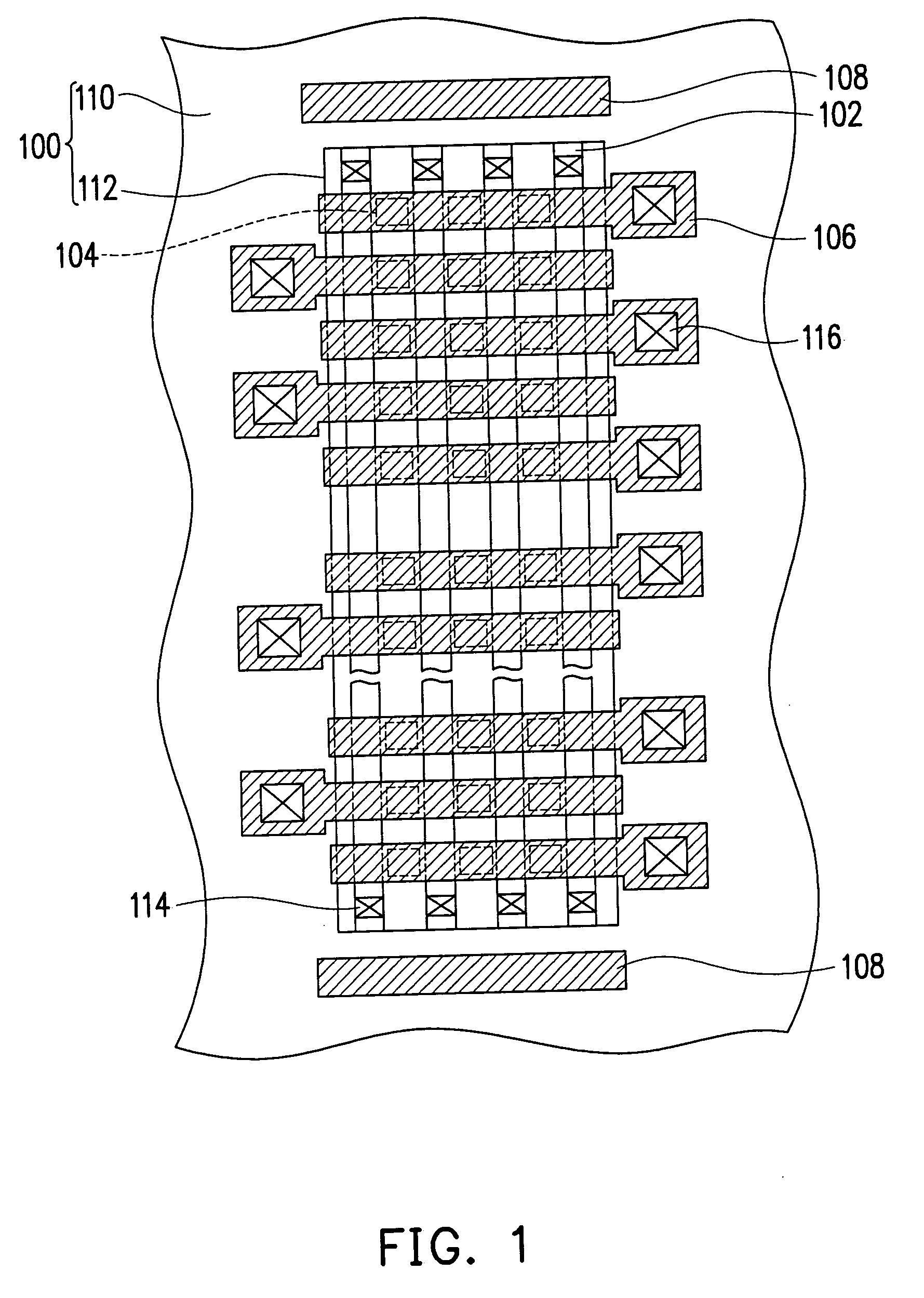
[0016]It is firstly noted that though each row of transistors / memory cells in the two embodiments illustrated by FIGS. I and 2 includes three transistors / memory cells, the number of transistors / memory cells in each row is not limited to three in this invention.

[0017]Referring to FIG. 1, the layout structure in this embodiment includes a substrate 100, bit lines 102 in the column direction, transistors 104 as memory cells, word lines 106 in the row direction and at least two dummy word lines 108, wherein the column direction is usually perpendicular to the row direction. The substrate 110 has therein an isolation structure 110, such as an STI structure or a FOX layer, which defines an active area 112. The bit lines 102 are disposed in the substrate 100 in the active area 112, each possibly being a linear doped region. The transistors 104 are disposed on the substrate 100 between the buried bit lines 102 and arranged in rows and columns. Each transistor 104 serves as a memory cell, an...


PUM


Abstract

A layout structure for non-volatile memory is described, including a substrate, bit lines in a column direction, transistors as memory cells, word lines in a row direction, bit line contacts and at least two dummy word lines. The substrate has therein an isolation structure that defines an active area. The bit lines are disposed in the substrate in the active area. The transistors are disposed on the substrate between the bit lines and arranged in rows and columns. Each word line is coupled to the transistors in one row. The bit line contacts are disposed on the bit lines. The dummy word lines are disposed on the isolation structure, respectively at two sides of the active area and parallel with the word lines.

Description

BACKGROUND OF THE INVENTION[0001]1. Field of the Invention[0002]The present invention relates to a semiconductor device layout structure. More particularly, the present invention relates to a layout structure of non-volatile memory.[0003]2. Description of the Related Art[0004]As microprocessors and software get more powerful, higher memory capacity is required. The memory capacity is raised mostly by increasing the integration degree of the memory device, so that the design rule of memory layout becomes narrower.[0005]There are many variation factors in a memory fabricating process that affect the yield and reliability of memory devices. For example, the critical dimension (CD) at edges of a memory array is easily different from that at the center of the same due to the lithographic optics, so that a malfunction like leakage or short circuit is often caused lowering the yield and reliability of the memory device. It is therefore important to uniformize the critical dimension in a me...

Claims


Application Information

Patent Timeline
IPC IPC(8): H01L29/94H01L23/52
CPCH01L27/115H10B69/00
Inventor KIM, JONGOHLIU, CHENG-JYE
Owner MACRONIX INT CO LTD
Why Eureka
Try Eureka