Method for developing processing

A processing method and developer technology, which is applied in the fields of electrical components, semiconductor/solid-state device manufacturing, circuits, etc., can solve the problem of developer reduction and other issues

Inactive Publication Date: 2010-12-22
TOKYO ELECTRON LTD
View PDF4 Cites 0 Cited by
  • Summary
  • Abstract
  • Description
  • Claims
  • Application Information

AI Technical Summary

Problems solved by technology

[0008] After the development reaction is completed, when pure water is supplied to the semiconductor wafer, the pH of the developer on the semiconductor wafer drops sharply, so the dissolved product solid is precipitated and attached to the developed pattern, which may cause defects

Method used


Image

  • Method for developing processing
  • Method for developing processing
  • Method for developing processing

Examples


Embodiment Construction

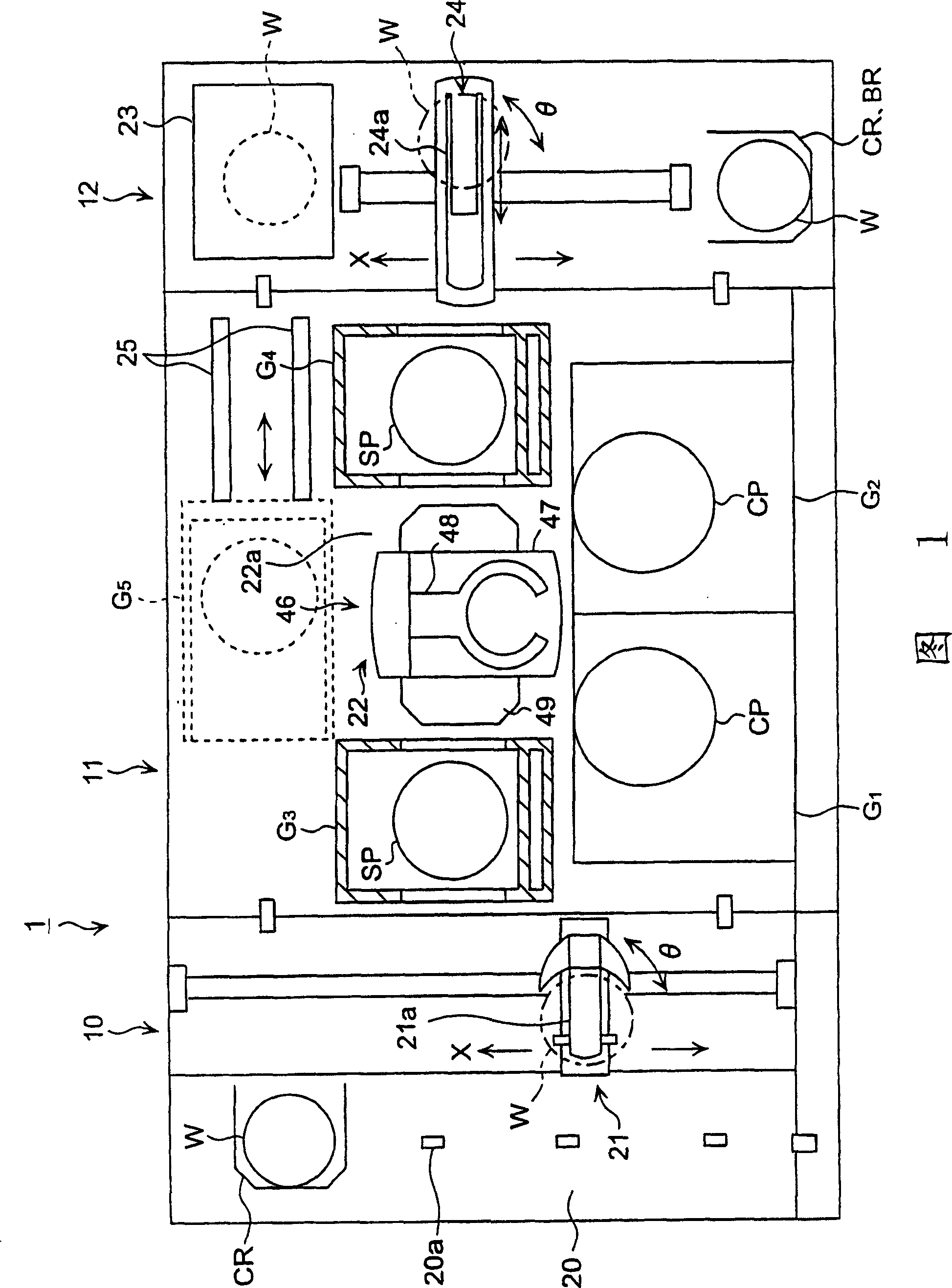
[0042] Embodiments of the present invention will be described in detail below with reference to the drawings. Here, a development treatment method using a resist coating development treatment system that continuously performs from application of a resist to a semiconductor wafer (wafer) to development treatment will be described.

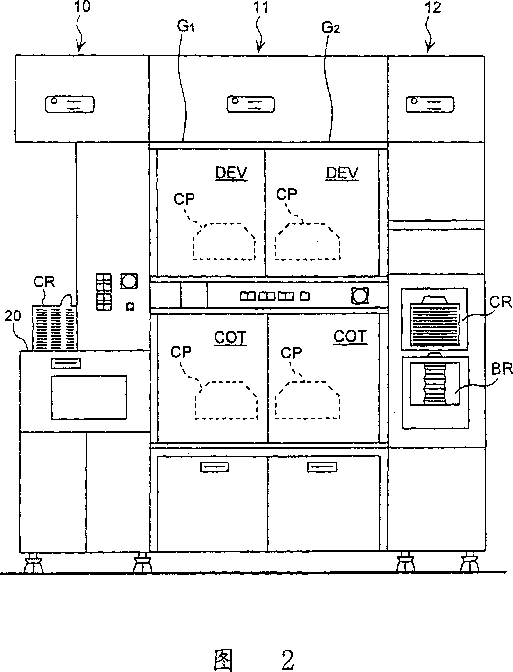
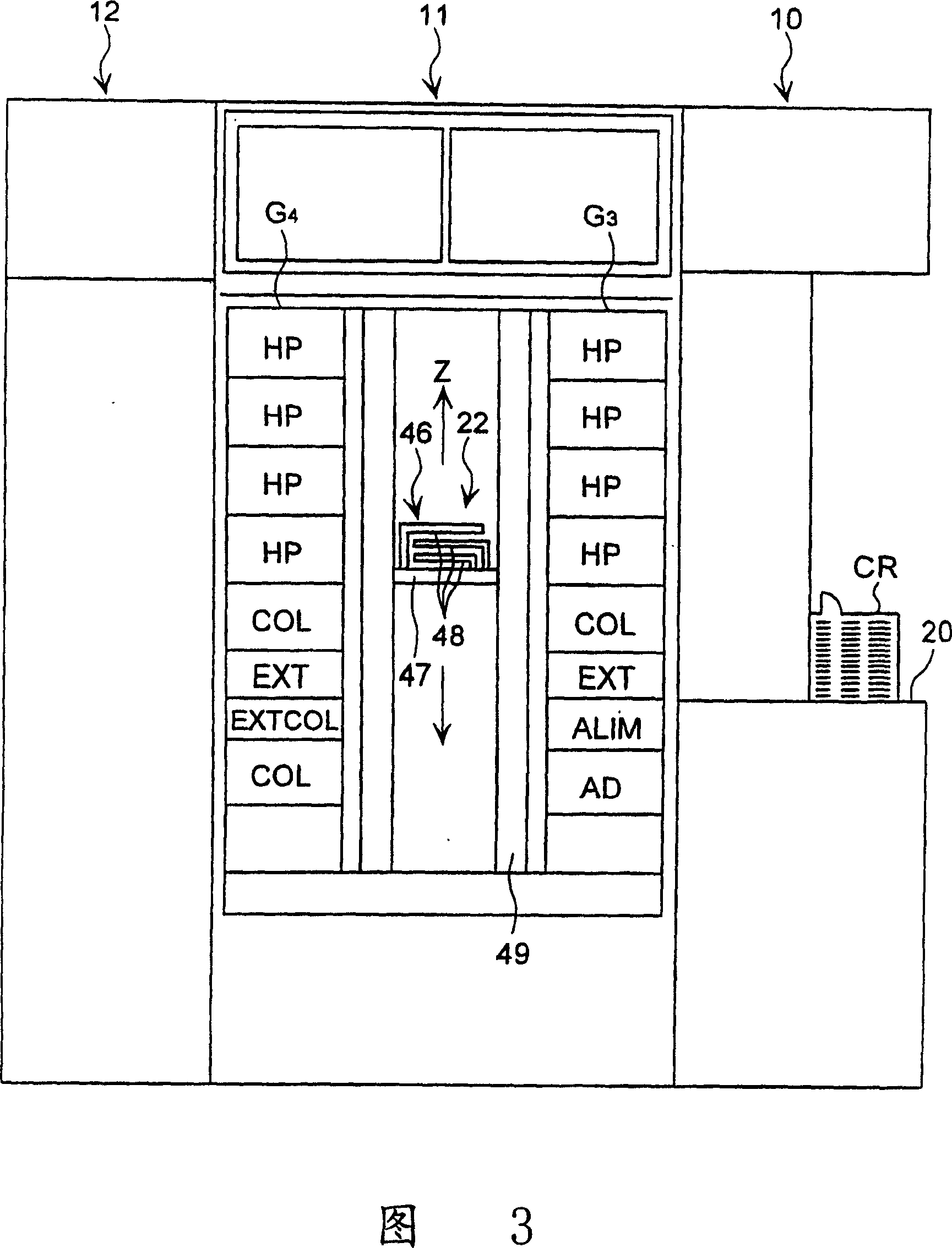
[0043] figure 1 is a schematic plan view showing a resist coating and development processing system, figure 2 is its front view, image 3 is its rear view. This resist coating and development processing system 1 has a box-type table 10 as a transfer table, a processing table 11 having a plurality of processing units, and a wafer W provided between and an exposure device not shown adjacent to the processing table 11. The interface part 12.

[0044] The box stage 10 carries out operation from another system to the present resist coating and developing processing system 1 in a state where a plurality of, for example, 25 wafers W as objects to be p...


PUM


Abstract

The invention provides a developing processing method of a resist film processed the exposure treatment on a substrate, which is characterized in that: the method comprises following steps: coating the developing solution on the substrate; laying the substrate of the developing liquid for a certain time for developing; coating the solution on the substrate which is coated with the developing solution, in which the solution is selected from TMAH solution with a mixing rate of 0.1-1.5% with the pure water, diluted developing liquid, pure water, aqueous solution with pH value 9-12 or hydrophilicorganic solution with pH value 9-12 when added with an interfacial agent in the pure water; laying the substrate coated with the liquid for a prescribed time to reduce the dissolution product concentration generated by the developing solution; rinsing the substrate coated with the liquid. The invention also provides a developing liquid coating device.

Description

[0001] This application is a divisional application of a Chinese patent application with the patent application number 02143756.4, the filing date being August 28, 2002, and the invention title being "Development Treatment Method and Developer Solution Coating Device". technical field [0002] The present invention relates to a development treatment method and a developer solution coating device for performing development treatment on a substrate such as an exposed semiconductor wafer. Background technique [0003] In the manufacturing process of semiconductor devices, a predetermined circuit pattern is formed on the surface of a semiconductor wafer using so-called photolithography. In this photolithography process, a series of processes such as applying a photoresist liquid on a cleaned semiconductor wafer to form a resist film, exposing the resist film in a predetermined pattern, and developing it are performed. [0004] In such a developing process, the semiconductor wafe...

Claims


Application Information

Patent Timeline
Patent Type & Authority Patents(China)
IPC IPC(8): G03F7/30G03F7/26
Inventor 吉原孝介田中启一山本太郎京田秀治竹口博史大河内厚
Owner TOKYO ELECTRON LTD
Why Eureka
Try Eureka