Chip bearing belt and chip packaging construction

A technology of chip packaging structure and carrying tape, which is applied in the direction of electrical components, electric solid devices, circuits, etc., and can solve problems that affect the reliability of the overall components, alignment difficulties, and chips that cannot be installed correctly

Inactive Publication Date: 2009-05-06
CHIPMOS TECH INC
View PDF0 Cites 1 Cited by
  • Summary
  • Abstract
  • Description
  • Claims
  • Application Information

AI Technical Summary

Problems solved by technology

This deformation may cause the chip carrier tape 1 to produce non-uniform deformation, and will generate shear stress between the polyimide substrate 11 and the copper layer 13, causing such as figure 1 warpage
[0004] This warping phenomenon will cause many disadvantages
For example, in the process of automatically installing chips on the chip carrier tape, if the chip carrier tape is warped to make it uneven, it will cause inaccurate positioning of the chip when installing the chip, resulting in the chip not being correctly installed on the chip carrier tape on, or even damage the chip or automation equipment
Or, if the chip carrier tape installed with the chip has warpage, it is not conducive to the subsequent application of the chip carrier tape. Due to warpage, problems such as difficult alignment, empty soldering or incomplete bonding will occur, which will affect the reliability of the overall component
Defective products with insufficient reliability will not be accepted by the market
[0005] From the above description, it can be known that in the prior art, the chip carrier tape often warps, which will cause the chip carrier tape to be uneven, thereby affecting the application of the chip carrier tape

Method used


Image

  • Chip bearing belt and chip packaging construction
  • Chip bearing belt and chip packaging construction
  • Chip bearing belt and chip packaging construction

Examples


Embodiment Construction

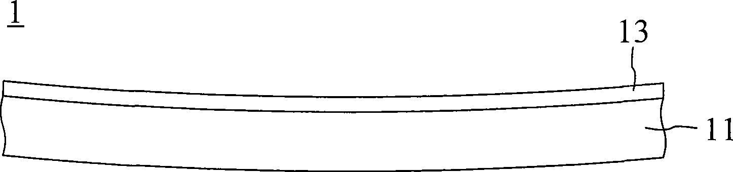
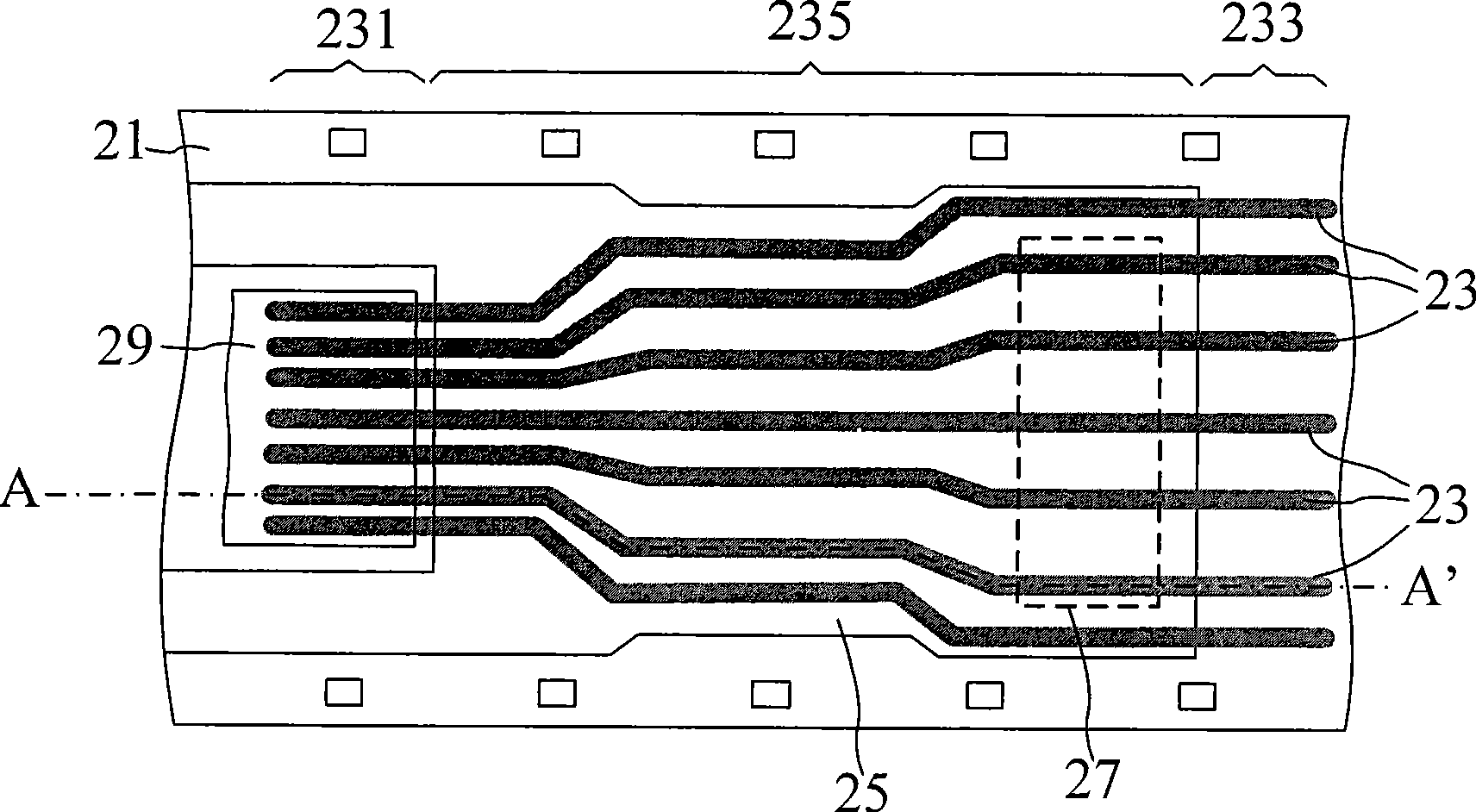
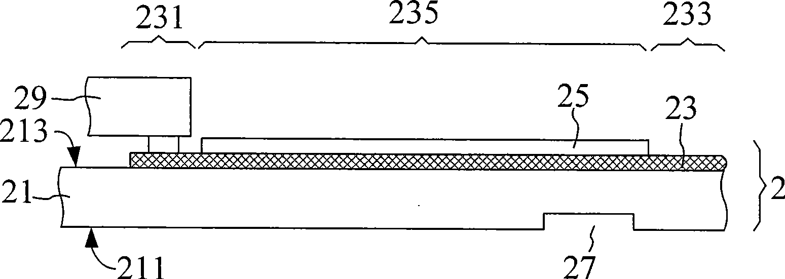
[0030] Also refer to Figure 2A and 2B ,in Figure 2A It is a schematic top view of the chip carrier tape 2 of the present invention, and Figure 2B for Figure 2A Sectional view at section line AA' in middle. The chip carrier tape 2 of the present invention includes a flexible substrate 21 , a patterned conductive layer 23 , and a solder resist layer 25 . The flexible substrate 21 is a polymer substrate, usually polyimide (PI) substrate. The flexible substrate 21 has a first surface 211 and a second surface 213 opposite to the first surface 211 . Wherein, a first recessed structure 27 is disposed on the first surface 211 . When the chip carrier tape 2 enters a low-temperature environment from a high-temperature environment (for example, after baking), because the flexible substrate 21 and the patterned conductive layer 23 have different thermal expansion coefficients (for example, the thermal shrinkage of metal copper is greater than that of polyamide imine), will lead...


PUM


Abstract

A bearing belt for a chip comprises a flexible substrate. The flexible substrate is provided with a first surface provided with a first depressed structure, a second surface opposite to the first surface, and a patterning conducting layer arranged on the second surface.

Description

technical field [0001] The invention relates to a chip carrying tape; specifically, the present invention is a chip carrying tape applicable to chip packaging. Background technique [0002] Currently known chip carrier tapes are mainly applicable to TCP (tape carrier package) or COF (chip on film) packaging of semiconductor components (such as chips). A commonly used chip carrier tape is mainly composed of a flexible substrate (such as a polyimide (PI) substrate) and a metal conductive layer (such as a copper layer). Currently, in the process of using the chip carrier tape, it is often found that the chip carrier tape is warped. This phenomenon is mainly due to the fact that the chip carrier tape itself is made of a composite structure of different materials. Not only is it a soft material, but also the different materials between the layers have different thermal expansion coefficients. During the packaging process, due to temperature changes, different degrees of expansi...

Claims


Application Information

Patent Timeline
Patent Type & Authority Applications(China)
IPC IPC(8): H01L23/498
Inventor 沈弘哲刘宏信
Owner CHIPMOS TECH INC
Why Eureka
Try Eureka