Micro-tip array device and its production method

A manufacturing method and micro-tip technology, which can be used in the manufacture of instrument parts, instruments, nanostructures, etc., can solve the problem of low working efficiency of single probe, achieve high-resolution nanoscale graphics processing and high-density data storage, The effect of reducing the area of ​​the connection unit and optimizing the structure

Inactive Publication Date: 2011-07-20
北京中科仁健科技有限公司
View PDF0 Cites 0 Cited by
  • Summary
  • Abstract
  • Description
  • Claims
  • Application Information

AI Technical Summary

Problems solved by technology

[0006] In view of this, the main purpose of the present invention is to provide a micro-tip array device and its manufacturing method, to realize high-resolution nanoscale pattern processing and high-density data storage, and solve the problem of low working efficiency of single probe

Method used


Image

  • Micro-tip array device and its production method
  • Micro-tip array device and its production method
  • Micro-tip array device and its production method

Examples


Embodiment Construction

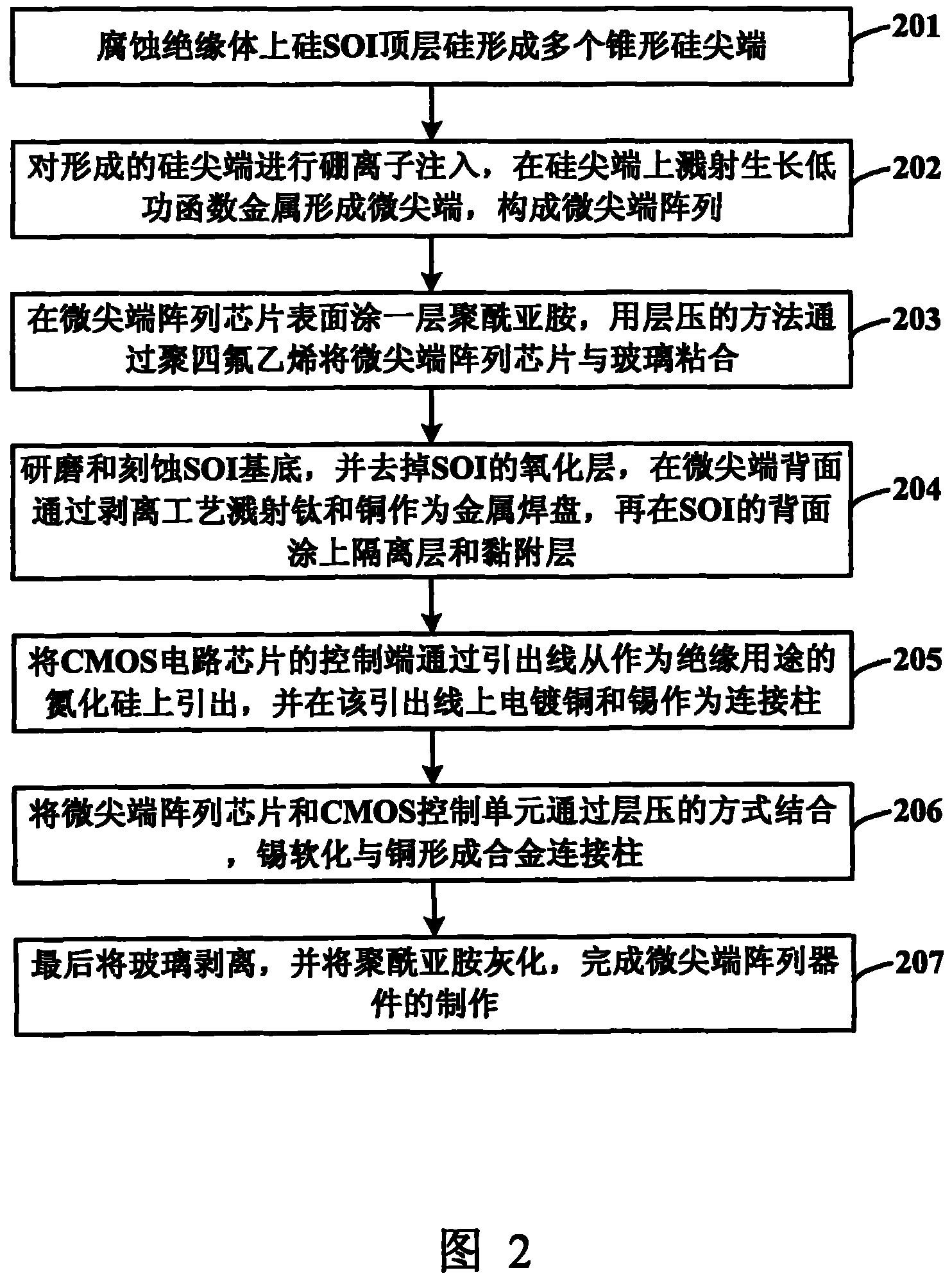
[0043] In order to make the object, technical solution and advantages of the present invention clearer, the present invention will be described in further detail below in conjunction with specific embodiments and with reference to the accompanying drawings.

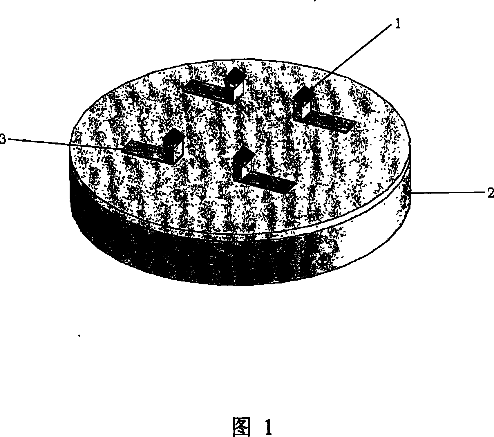
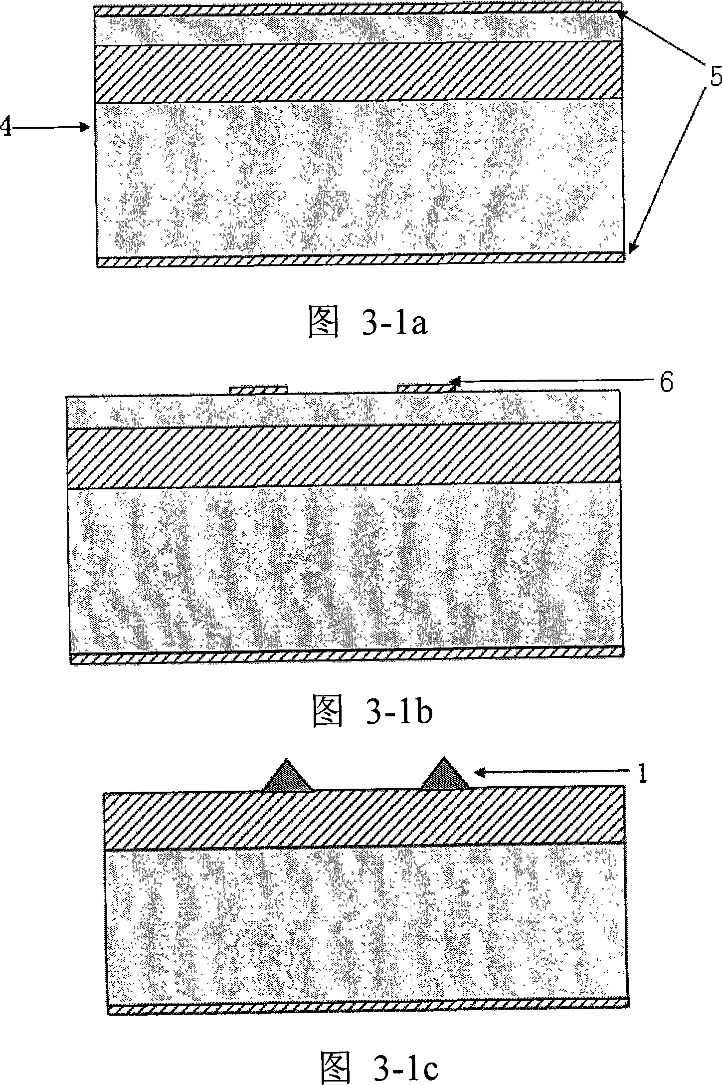
[0044] The micro-tip in the present invention utilizes the low-energy electron beam emitted by the metal tip under the field emission effect for graphic processing. Since the electron beam can effectively avoid the proximity effect, the resolution of the processed graphic can be improved and nano-scale graphics can be realized. Processing, and the processing speed can be improved by arraying the tip.

[0045] The invention proposes to use the connection column to realize the mechanical and electrical connection between the CMOS control circuit unit and the micro-tip array chip, effectively reduces the area of ​​the connection line by utilizing the space, and improves the integration degree of the device.

[0046] Such as ...


PUM


Abstract

The invention relates to the technical fields of deep sub-micron and nano processing in the microelectronic technology, and discloses a microtip array device. The device is composed of a microtip array, a COMS control circuit unit and connection columns; the microtip array comprises a plurality of microtips, each microtip is mechanically and electrically connected with the COMS control circuit unit by a connection column; the COMS control circuit unit is used for controlling the microtips in the microtip array to operate independently; and the connection columns are used for realizing mechanical and electrical connection between the microtips and the COMS control unit in the microtip array. The invention further discloses a manufacturing method of the microtip array device. The COMS circuit controls metal tip field emission electron beams by the microtip array device and the manufacturing method to realize high-resolution nano-scale graphical processing and high-density data storage, and the problem of low operating efficiency of a single probe is solved by the microtip array.

Description

technical field [0001] The invention relates to the technical field of deep submicron and nano processing in microelectronic technology, in particular to a microtip array device based on the field electron emission effect and a manufacturing method thereof. Background technique [0002] Since the invention of the tunneling microscope (STM) by G. Bining and others of IBM Corporation in 1982, various micro-tip devices have emerged at home and abroad. These devices have been widely used in material surface detection, high-density data access, ultra-fine graphics processing and many other aspects. [0003] At present, the technologies used in high-density information storage and graphic processing of micro-tip devices are mainly: electrothermal method, direct scribing method and electric field processing method. Electrothermal writing uses the heat flow emitted by the tip to soften the medium to produce graphics. The direct scribing method is to use the cutting-edge mechanical...

Claims


Application Information

Patent Timeline
Patent Type & Authority Patents(China)
IPC IPC(8): G12B21/00G12B21/02G11B13/08G11B11/24B82B3/00
Inventor 陈大鹏傅剑宇景玉鹏欧毅叶甜春
Owner 北京中科仁健科技有限公司
Why Eureka
Try Eureka