System for initially generating stabilized in-chip clock
A technology for initializing and stabilizing chips, applied in the directions of signal generation/distribution, automatic power control, electrical components, etc., which can solve the problems of increasing process costs and expensive test steps, reducing costs, simplifying the trimming process, and avoiding the test environment. Effects of use with test equipment
- Summary
- Abstract
- Description
- Claims
- Application Information
AI Technical Summary
Problems solved by technology
Method used
Image
Examples
Embodiment 1
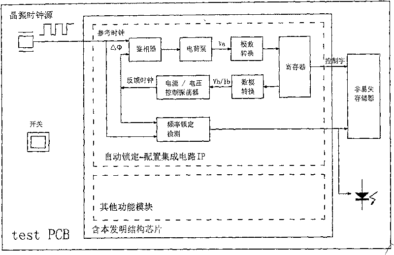
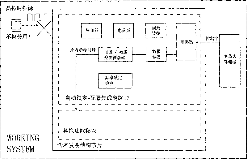
[0021] like Figure 1-2 As shown, a system for initializing and generating a stable on-chip clock includes a chip provided with an automatic clock-locking-configuration integrated circuit IP, a crystal oscillator clock source, a non-volatile memory, and a light-emitting diode. The automatic clock-locking-configuration integration The circuit IP includes a phase detector, a charge pump, an analog-to-digital converter, a register, a digital-to-analog converter, a current / voltage control oscillator and a frequency lock detection circuit, the crystal oscillator clock source is connected to one end of the phase detector, and the phase detector The output of the device is connected to the input of the charge pump, the output of the charge pump is connected to the input of the analog-to-digital converter, the output of the analog-to-digital converter is connected to the input of the register, and the register is also connected to the digital-to-analog converter and the non-volatile me...
Embodiment 2
[0031] This solution is a PCB version-level application solution that uses clock automatic locking-configuration integrated circuit IP to complete initialization and generate stable on-chip clock.
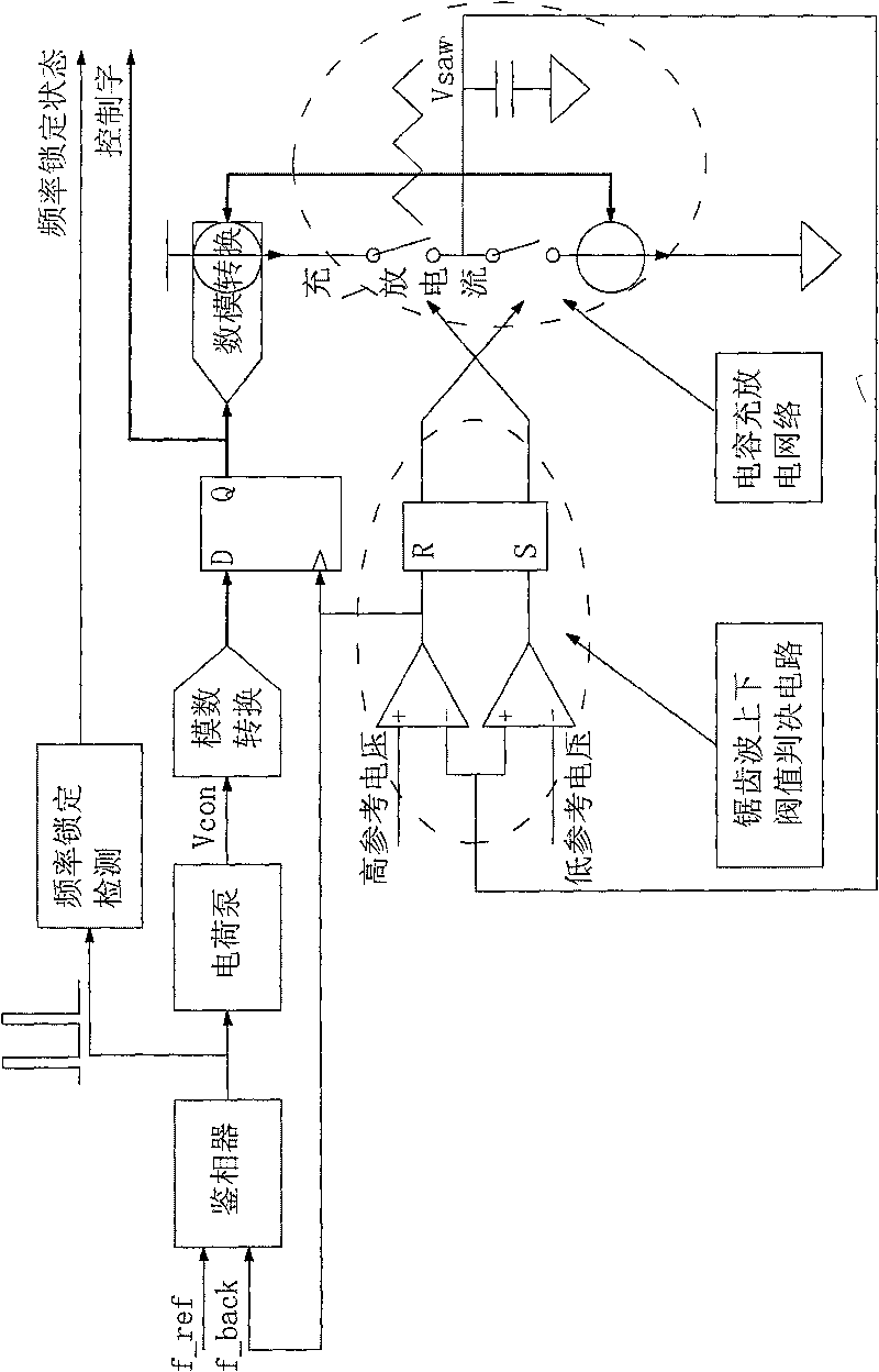
[0032] like image 3 As shown, a specific initialization circuit:
[0033] The crystal reference clock f_ref and the feedback clock f_back are input to the phase detector as two input signals, and the phase detector outputs the two signals to the charge pump, the charge pump outputs the signal to the analog-to-digital converter, and the analog-to-digital converter outputs the signal to DFF data input, feedback clock f_back output to DFF clock input, DFF stores the conversion result of the analog-to-digital converter on each rising edge of the feedback clock f_back and outputs it to the digital-to-analog converter, and the output current of the digital-to-analog converter is used as a capacitor charging and discharging network Charge / discharge current, capacitor charge and discharg...
PUM
 Abstract
Description
Claims
Application Information


