Photomask, manufacturing method thereof, and pattern transfer print method

A mask pattern and manufacturing method technology, applied in the field of photomasks, can solve the problems of electrostatic damage, static electricity generated by shading patterns, and increased damage, and achieve the effect of suppressing electrostatic damage

Inactive Publication Date: 2009-05-27
HOYA CORP
View PDF2 Cites 20 Cited by
  • Summary
  • Abstract
  • Description
  • Claims
  • Application Information

AI Technical Summary

Problems solved by technology

[0004] In addition, it is known that there is a problem in the photomask used in the manufacture of semiconductor devices: static electricity is generated in the light-shielding pattern, a potential difference is generated between electrically independent patterns, and electrostatic breakdown is caused by discharge. The method of the invention described in JP-A-2003-248294 (Patent Document 2) uses dummy patterns to electrically connect t

Method used


Image

  • Photomask, manufacturing method thereof, and pattern transfer print method
  • Photomask, manufacturing method thereof, and pattern transfer print method
  • Photomask, manufacturing method thereof, and pattern transfer print method

Examples


Embodiment Construction

[0044] Hereinafter, the best mode for carrying out the present invention will be described with reference to the drawings.

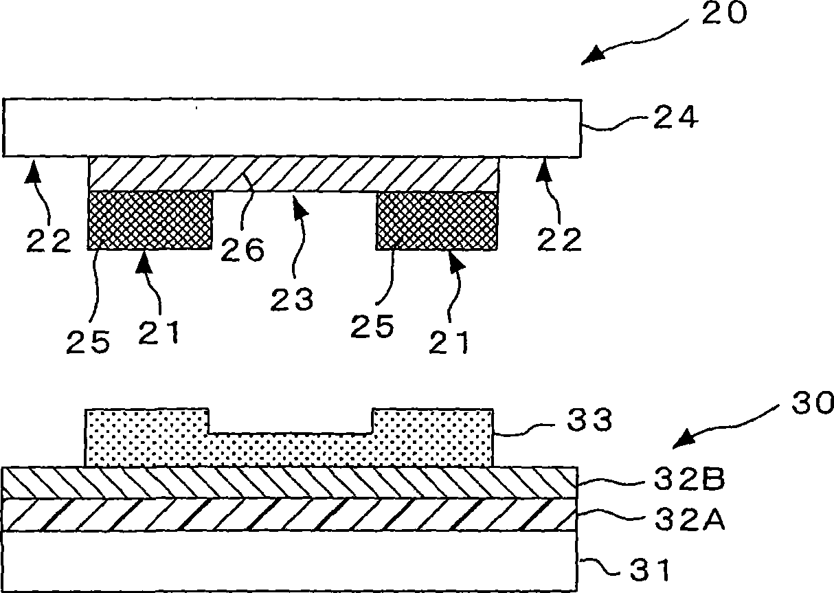
[0045] figure 1 It is a sectional view for explaining the pattern transfer method using the gray scale mask which is one embodiment of this invention. figure 1 The grayscale mask 20 shown is used to form a resist pattern 33 having a film thickness stepwise different on the transfer target body 30 . In addition, in figure 1 In , symbols 32A and 32B denote films laminated on the substrate 31 in the body to be transferred 30 .

[0046] figure 1 The grayscale mask 20 shown has a mask pattern on a transparent substrate 24, and the mask pattern is formed by a light shielding portion 21 that shields exposure light (the transmittance is about 0%) when the grayscale mask 20 is used. , the translucent part 22 through which the exposure light exposed on the surface of the transparent substrate 24 passes, and the translucent part which reduces the transmitta...


PUM


Abstract

The invention provides a photomask, a method for manufacturing the photomask, and a pattern transfer method. An object of the invention is to provide a photomask such as a gray mask, which can restrain electrostatic destruction of pattern caused in treatment in mask use, even if electrostatic destruction is generated, mask design formed by an apparatus may not be affected in use. According to the invention, a photomask is provided on a transparent substrate (24) for forming desired mask patterns of the transfer patterns (such as gray masks), and conductive patterns separately guided from separated a plurality of mask designs (11a and 11b, 11c and 11d, 12a and 12b, 12c and 12d) are provided. The conductive patterns have non-contact parts nearer each other in comparison with each space between each mask pattern, which is formed by such as semitranslucent film or translucent film.

Description

technical field [0001] The present invention relates to a pattern transfer method for forming a transfer pattern on a photoresist on a body to be transferred using a mask, a photomask used in the pattern transfer method, and a manufacturing method thereof. Background technique [0002] Now, in the field of liquid crystal display (Liquid Crystal Display: hereinafter referred to as LCD), thin film transistor liquid crystal display (Thin Film Transistor Liquid Crystal Display: hereinafter referred to as TFT-LCD), compared with CRT (cathode line tube) , due to the advantages of being easy to make thin and low power consumption, it is now being rapidly commercialized. TFT-LCD has a TFT substrate with a structure in which TFTs are superimposed on each pixel arranged in a matrix under the intervention of a liquid crystal phase, and a color filter in which red, green, and blue pixel patterns are arranged corresponding to each pixel schematic structure. In the TFT-LCD, there are ma...

Claims


Application Information

Patent Timeline
IPC IPC(8): G03F1/14G03F1/00G03F7/00G03F1/40G03F1/68G03F1/80H01L21/027
CPCG03F1/32
Inventor 佐野道明
Owner HOYA CORP
Why Eureka
Try Eureka