Check patentability & draft patents in minutes with Patsnap Eureka AI!

Semiconductor non-volatile memory

一种非易失性、半导体的技术,应用在静态存储器、只读存储器、信息存储等方向,能够解决增加升压电路、消耗电流增加、妨碍系统高速化等问题,达到高速化访问、减少功耗的效果

Inactive Publication Date: 2009-05-27
PANASONIC CORP
View PDF7 Cites 0 Cited by
  • Summary
  • Abstract
  • Description
  • Claims
  • Application Information

AI Technical Summary

Problems solved by technology

Also, after that, it is necessary to continuously activate only the select gates required to read
[0024] That is, there is a problem that a discharge period for discharging each bit line to ground is necessary in the read operation.
In addition, there is a problem that the current consumption required to activate all the selection signals for the selected sector increases, and because the level of the selection signal is different, it is necessary to increase the problem of a booster circuit.
[0025] As described above, in the prior art, it is necessary to provide a period for each bit line in the discharge sector before the read operation of the memory cell, so this becomes a factor that hinders the speed-up of the system.
In addition, there is a problem that the current consumption of the circuit increases due to the discharge operation, and when the boost power supply is used for the discharge operation, there is a problem that the chip area increases due to the increase in the area of ​​the boost circuit.

Method used


Image

  • Semiconductor non-volatile memory
  • Semiconductor non-volatile memory
  • Semiconductor non-volatile memory

Examples


Embodiment approach 1

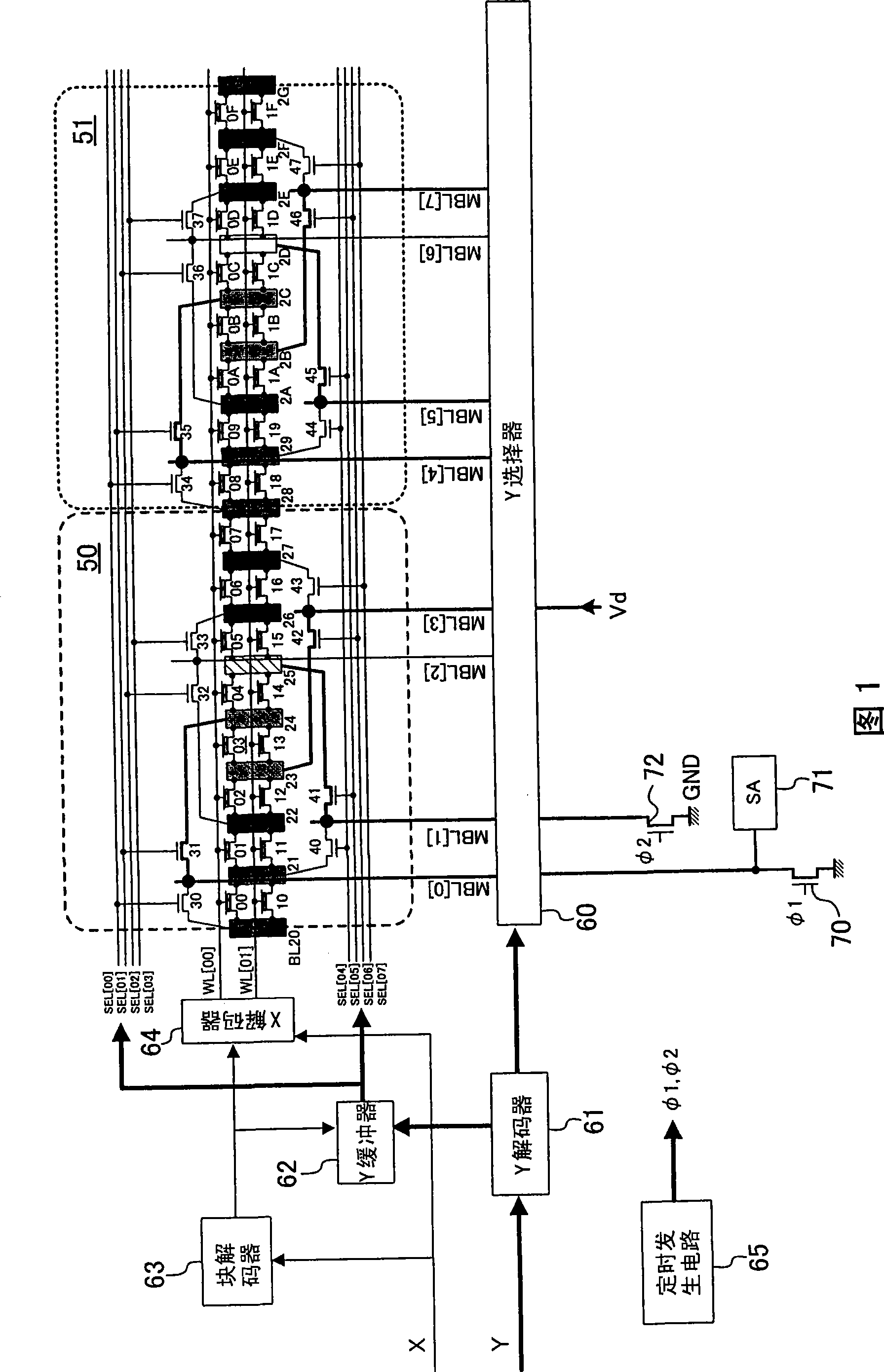
[0056] FIG. 1 is a diagram showing the configuration of a semiconductor nonvolatile memory according to Embodiment 1 of the present invention.

[0057] The semiconductor nonvolatile memory shown in FIG. 1 is a VGA (Virtual Ground Architecture) type, in which memory cells are arranged continuously between bit lines, and adjacent memory cells share bit lines. 00 to 0F and 10 to 1F are memory cells, BL20 to 2G are bit lines, and these constitute a memory cell array. For example, bit line BL24 is connected to both the source of memory cell 03 and the drain of memory cell 04 .

[0058] Moreover, in FIG. 1, WL[00]~[01] are word lines, MBL[0]~[7] are main bit lines, 30~37, 40~47 are selected according to the selection gate signal SEL[00]~ [07] The selection gates of the bit lines BL20-2G and the main bit lines MBL[0]-[7] are selectively connected. Also, 63 is a block decoder that accepts an X address and activates a sector, 64 is an X decoder that receives an X address and activate...

Embodiment approach 2

[0076] 4 is a diagram showing the structure of a semiconductor nonvolatile memory according to Embodiment 2 of the present invention. In FIG. 4 , the same reference numerals as those in FIG. 1 are assigned to components common to those in FIG. 1 , and detailed description thereof will be omitted here.

[0077] The semiconductor nonvolatile memory of FIG. 4 includes, in addition to the configuration of FIG. 1 , a proximity effect compensator unit NEC as a circuit element used for reading. The proximity effect compensator unit NEC includes a proximity bit line reset transistor 73 and a current source 74 that flows a current smaller than the ON current of the memory cell. The current of the power source 74 is adjusted to be equal to the reference current, that is, approximately half of the current when the memory cell is "1". The same control signal Φ1 as that of the read input reset transistor 70 is given to the adjacent bit line reset transistor 73 . Y selector 60 a is config...

Embodiment approach 3

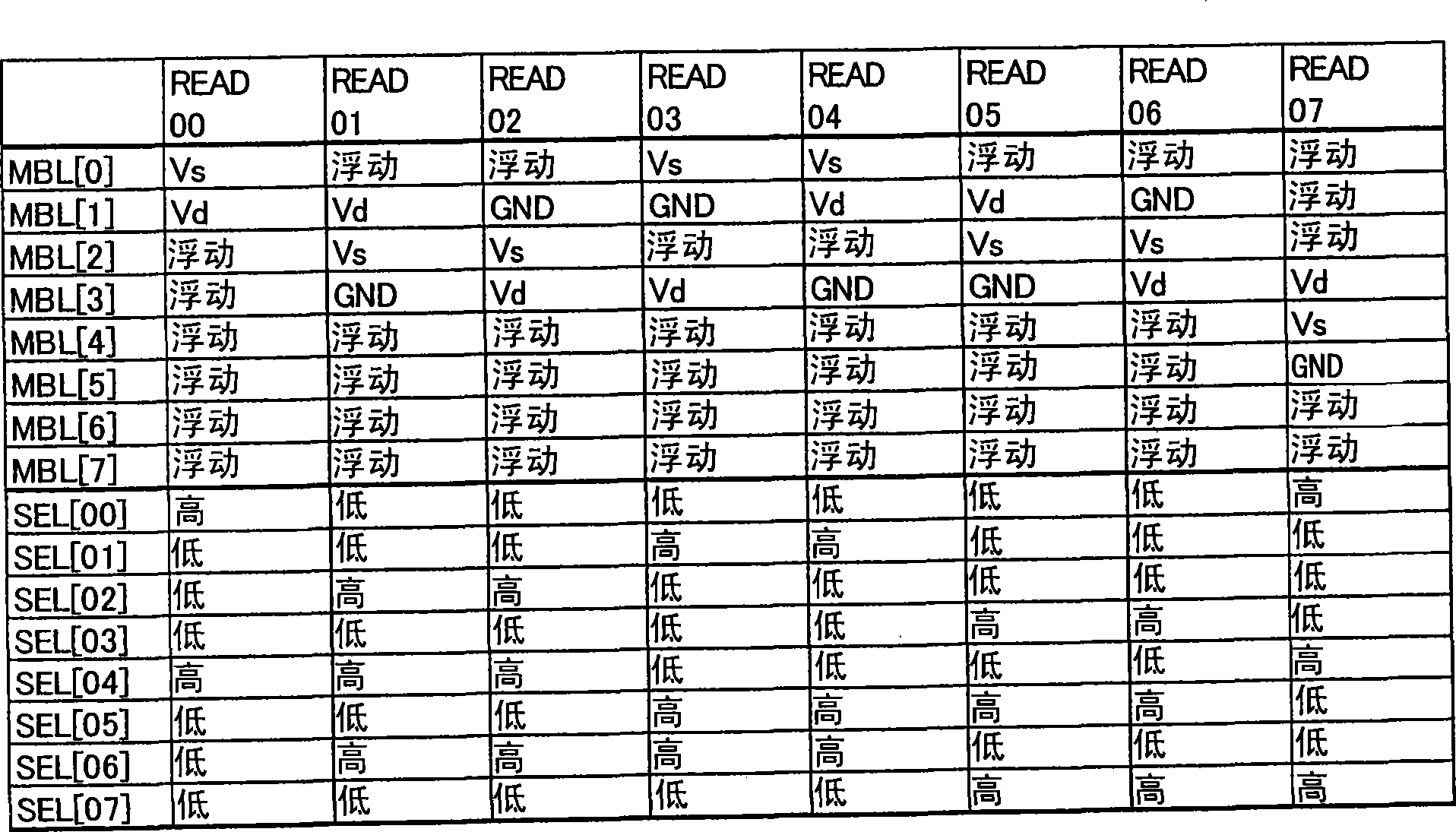
[0093] The configuration of the semiconductor nonvolatile memory according to Embodiment 3 of the present invention is the same as that of FIG. 1 . In this embodiment, the bit line adjacent to the drain bit line on the side opposite to the source bit line is forced to be at the ground potential also during reading of the memory cell. For example, when reading the memory cell 03, the bit line BL22 connected to the drain of the memory cell 02, which is the third memory cell having the drain bit line BL23 connected to the source, is also connected to the ground power supply GND. . Other operations are the same as in Embodiment 1.

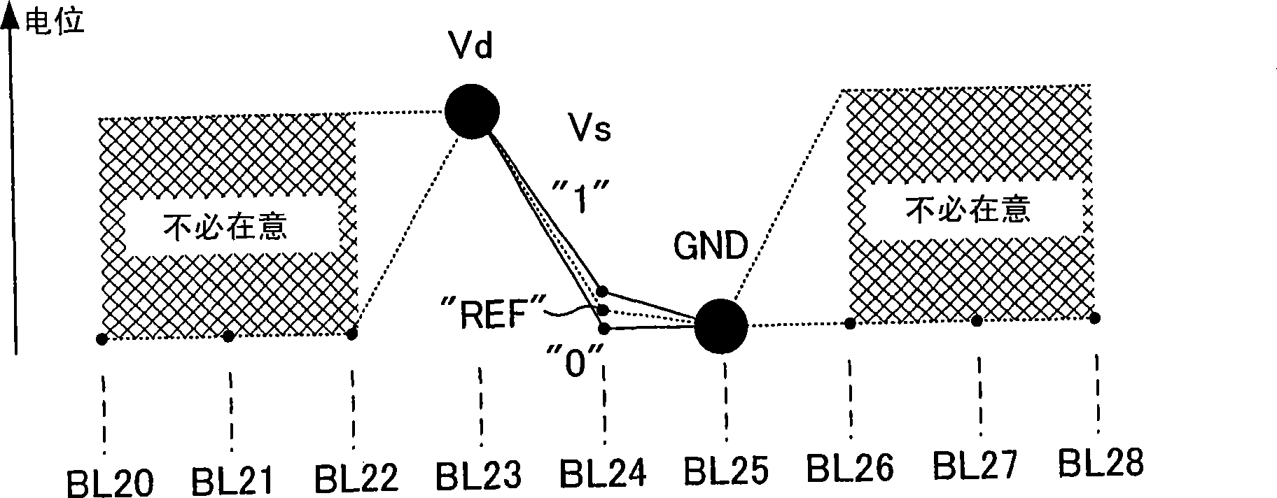
[0094] Figure 7 It is a diagram showing how the potential of the bit line near the memory cell 03 is read when the integration period ends in the present embodiment. Such as Figure 7 As shown, the bit line BL22 adjacent to the drain bit line BL23 on the side opposite to the source bit line BL24 is at ground potential.

[0095] If the bit line BL...


PUM


Abstract

The invention provides a semiconductor non-volatile memory, wherein a memory cell can be read accurately without having to discharge bit lines before the read operation. When reading a memory cell, the first bit line connected to the drain thereof is connected to the voltage source to receive a predetermined voltage, and the second bit line connected to the source thereof is connected to the sense amplifier. In this process, the third bit line in the vicinity of the second bit line is connected to the ground power supply. Thus, since the third bit line in the vicinity of the second bit line being sensed is forcibly set to the ground level, no charge flows in therefrom, thus preventing a current flowing into the second bit line.

Description

technical field [0001] The present invention relates to semiconductor non-volatile memories, and more particularly to circuit structures involved in the readout of memory cells. Background technique [0002] Semiconductor non-volatile memories are getting smaller and larger. Among them, in high-speed applications, a VGA (Virtual Ground Architecture, virtual ground) type semiconductor nonvolatile memory, which is one of the NOR types, is often used in terms of integration. In this VGA type, memory cells are arranged without interruption between all bit lines, and adjacent memory cells share bit lines with each other, which can roughly realize the 4F 2 The refinement of the scaling law. [0003] However, in this VAG type, since adjacent memory cells share the bit line, by applying a drain voltage to the read memory cell (albeit slightly, by reading the source voltage of the memory cell), the Charges are successively accumulated on the bit lines on which the read memory cell...

Claims


Application Information

Patent Timeline
Patent Type & Authority Applications(China)
IPC IPC(8): G11C16/26
CPCG11C16/26G11C16/0491
Inventor 小岛诚
Owner PANASONIC CORP
Features
  • R&D
  • Intellectual Property
  • Life Sciences
  • Materials
  • Tech Scout
  • Unparalleled Data Quality
  • Higher Quality Content
  • 60% Fewer Hallucinations
Learn More