Structure of low thermal resistance LED and method for producing the same

A technology of light-emitting diodes and light-emitting chips, which is applied to electrical components, electrical solid-state devices, circuits, etc., can solve problems such as reducing thermal resistance, and achieve the effects of reducing thermal resistance, improving service life, and increasing diffusion channels.

Inactive Publication Date: 2009-05-27
HC SEMITEK CORP
View PDF5 Cites 16 Cited by
  • Summary
  • Abstract
  • Description
  • Claims
  • Application Information

AI Technical Summary

Problems solved by technology

However, the structure of the above-mentioned LED light-emitting chip does n

Method used


Image

  • Structure of low thermal resistance LED and method for producing the same
  • Structure of low thermal resistance LED and method for producing the same
  • Structure of low thermal resistance LED and method for producing the same

Examples


Embodiment Construction

[0034] The structure and manufacturing method of a low thermal resistance light emitting diode chip of the present invention will be further described below with reference to the accompanying drawings and embodiments.

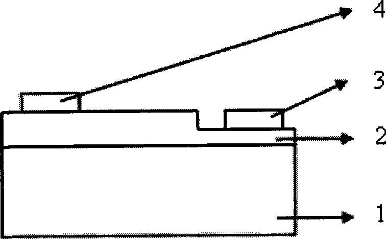
[0035] figure 1 Marks in: 1-Sapphire substrate, 2-Epitaxial layer, 3-N electrode, 4-P electrode;

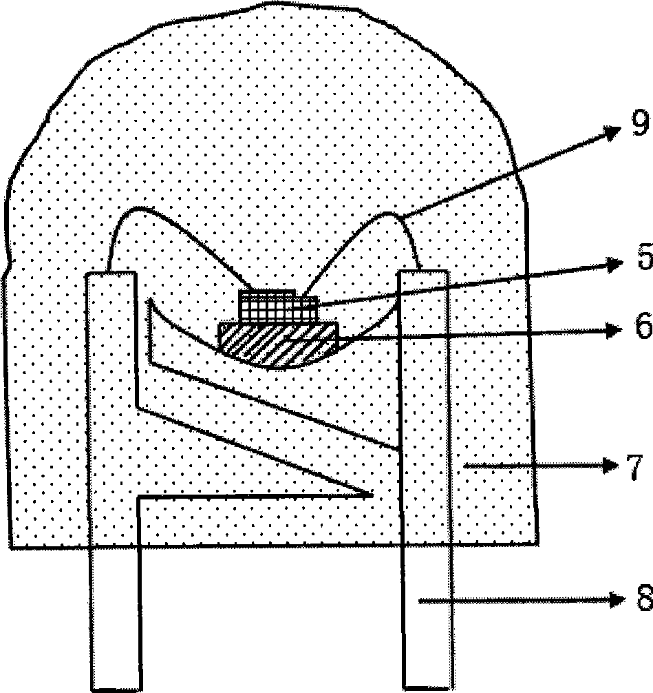
[0036] Figure 2A Marks in: 5-LED light-emitting chip, 6-adhesive, 7-epoxy, 8-bonding bracket, 9-gold wire;

[0037] image 3 The mark in: 10-low thermal resistance base, 11-metal reflective layer;

[0038] Figure 4 Mark in: 12-solder, 13-low thermal resistance heat sink substrate;

[0039] Figure 5A Mark in: 14-paraffin, 15-accompanying film;

[0040] The drawings used above are schematic diagrams, which are not drawn according to normal scale, but will not affect the understanding of the features and beneficial effects of the present invention by those skilled in the art.

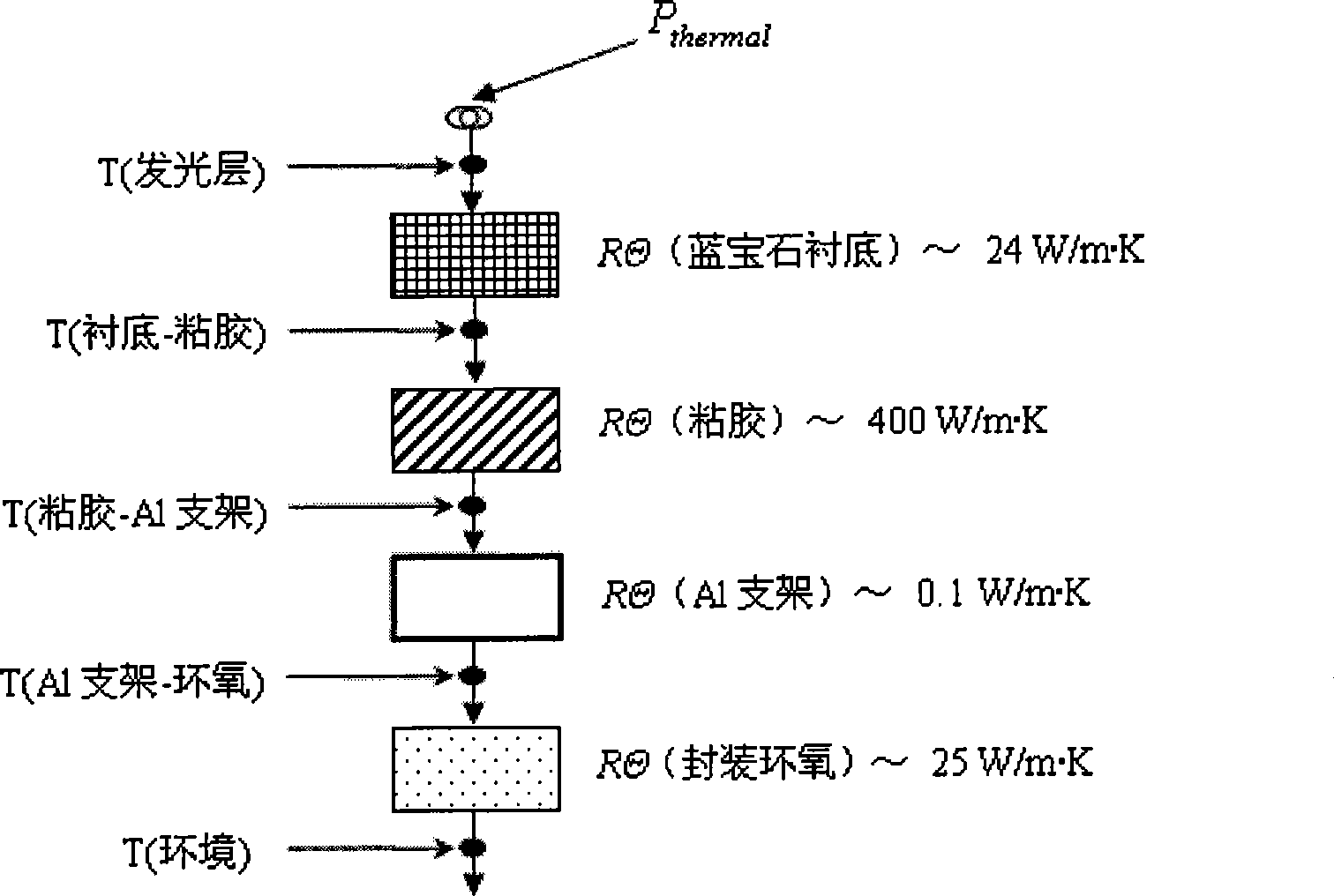
[0041] Figure 4 The structure of the low thermal resistance LED light-emitting chip...


PUM

PropertyMeasurementUnit
Thermal conductivityaaaaaaaaaa
Thicknessaaaaaaaaaa

Abstract

The invention provides a structure for a low thermal resistance LED chip and a method for manufacturing the same. The LED chip comprises P and N electrodes used for manufacturing electrodes, the LED luminous chip on a semiconductor epitaxial layer and a sapphire substrate, and a metallic reflector layer deposited on the bottom of the thinned sapphire substrate. The structure is characterized in that the LED chip comprises: (a) a heat radiating substrate with low thermal resistance, in which the size is larger than that of the LED luminous chip; and (b) solder deposited on the heat radiating substrate with low thermal resistance connected with the bottom of the metallic reflector layer. The area of the heat radiating substrate with low thermal resistance is 2 to 25 times larger than the area of the LED luminous chip. The invention can increase the area of heat dissipation channel when the LED luminous chip, significantly reduce thermal resistance of the LED luminous chip and packaged devices, reduce the light decay of LED devices and drain current, and prolong the life service of the devices.

Description

Technical field [0001] The invention relates to a manufacturing method of a light emitting diode chip, in particular to a structure of a low thermal resistance light emitting diode chip and a manufacturing method thereof, and belongs to the field of semiconductor optoelectronic devices. Background technique [0002] Light Emitting Diode (LED for short) is a solid-state semiconductor optoelectronic device that can directly convert electricity into light, which is called the fourth revolution of human lighting. LED lighting has the advantages of long life (over 100,000 hours), high efficiency, energy saving, environmental protection, and intelligence. LEDs are currently widely used in indoor and outdoor full-color displays, mobile phone backlights, traffic lights, indicator lights, special lighting, and landscape lighting. With the continuous improvement of LED luminous efficiency, high-brightness GaN LEDs are used in LCD backlights. High-end applications such as energy sources, st...

Claims


Application Information

Patent Timeline
IPC IPC(8): H01L33/00H01L33/60H01L33/64
CPCH01L2224/48091H01L2224/48247H01L2224/48257H01L2224/49107H01L2224/73265H01L2924/181
Inventor 刘榕董彬忠
Owner HC SEMITEK CORP
Why Eureka
Try Eureka