Semiconductor device and method for forming the same

A semiconductor and device technology, applied in the field of semiconductor devices and their formation, to achieve the effect of reducing the problem of noise coupling

Active Publication Date: 2009-06-10
SEMICON MFG INT (SHANGHAI) CORP
View PDF1 Cites 5 Cited by
  • Summary
  • Abstract
  • Description
  • Claims
  • Application Information

AI Technical Summary

Problems solved by technology

[0007] The problem solved by the present invention is to provide a semiconductor device, which can reduce the noise coupling problem of the semiconductor substrate in the hybrid circuit by implanting n-type ions only in the region where the n-type MOS transistor is located to form a deep n-type doped well

Method used


Image

  • Semiconductor device and method for forming the same
  • Semiconductor device and method for forming the same
  • Semiconductor device and method for forming the same

Examples


Embodiment Construction

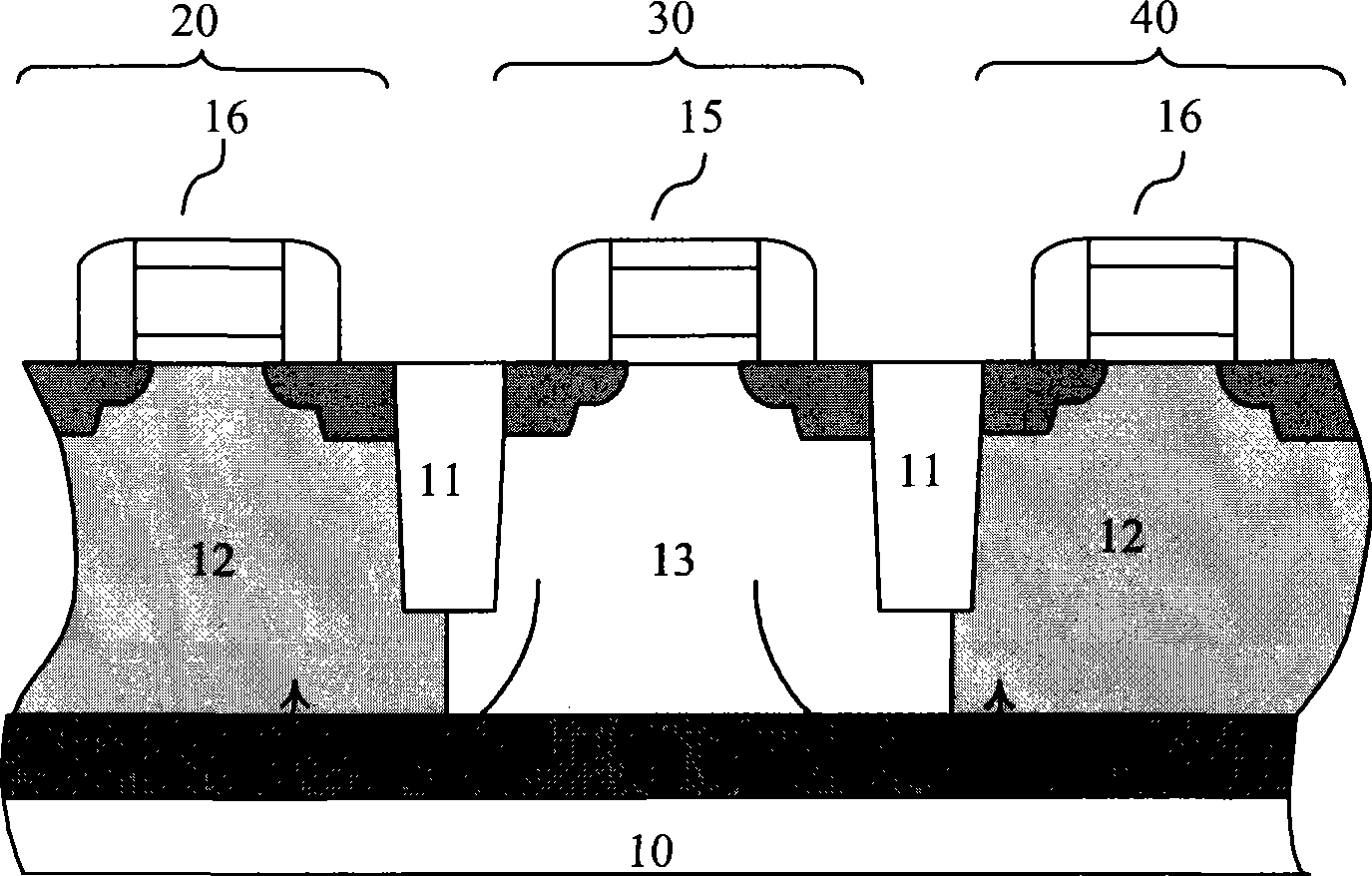
[0026] The present invention provides a semiconductor device. By forming a deep n-type doped well only in the region where the NMOS transistor is located in the semiconductor substrate, the longitudinal isolation of the NMOS transistor and the semiconductor substrate and the lateral isolation of the PMOS transistors on both sides are realized, reducing the Minimizes noise coupling problems in semiconductor substrates in hybrid circuits.

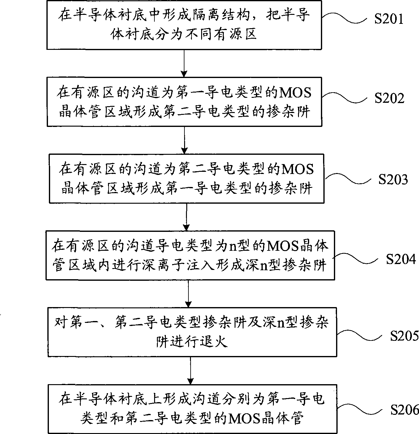
[0027] refer to figure 2 , first provide a schematic flow chart of forming the semiconductor device, including the following steps: performing step S201, forming an isolation structure in the semiconductor substrate, and dividing the semiconductor substrate into different active regions; performing step S202, forming an isolation structure in the active region. Forming a doped well of the second conductivity type in the MOS transistor region of the first conductivity type in the channel; performing step S203, forming a doped well of the firs...


PUM


Abstract

The invention provides a semiconductor device, which comprises an isolation structure which is positioned in a semiconductor substrate, a deep n-type doping well which is positioned in an MOS transistor region of n channel-conductive type in an active area, as well as an n-type MOS transistor which is formed on the semiconductor substrate, wherein the deep n-type doping well is positioned under a p-type doping well in the region and is electrically connected with n-type doping wells on two sides, and the ion doping concentration peak value of the deep n-type doping well and the doping ion concentration of the n-type doping wells at equal depth are equal in range. The invention also provides a method for forming the semiconductor device. By forming the deep n-type doping well in the region where the n-type MOS transistor is in the semiconductor substrate, the method realizes the longitudinal isolation of the n-type MOS transistor and the semiconductor substrate, as well as the transverse isolation of the semiconductor devices on two sides, and reduces the noise coupling in a hybrid integrated circuit.

Description

technical field [0001] The present invention relates to semiconductor devices and methods of forming them. Background technique [0002] With the development of modern CMOS technology, high-speed digital circuits and high-performance analog circuits can be integrated to form a mixed-signal integrated circuit, that is, a single-chip system (SoC). However, in the hybrid circuit, due to the large switching transient current in the digital state, disturbing charges are formed, and these disturbing charges can be coupled into sensitive analog circuits through the semiconductor substrate, forming background noise and causing interference. [0003] Shrinking semiconductor geometries have made noise coupling to the floor a significant problem for designers of new, more highly integrated SoCs. At present, the "triple well" process is generally used to reduce interference by adding deep n-type doped wells in the semiconductor substrate. [0004] figure 1 It is a schematic diagram o...

Claims


Application Information

Patent Timeline
Patent Type & Authority Applications(China)
IPC IPC(8): H01L21/8238H01L21/76H01L27/092
Inventor 赵猛
Owner SEMICON MFG INT (SHANGHAI) CORP
Why Eureka
Try Eureka