Optimized making method based on flat-plate wave guide mobile afebrile array wave guide grating

A technology of arrayed waveguide grating and slab waveguide, which is applied in the coupling of optical waveguide, etc., to achieve the effect of reducing production difficulty and production cost, reducing the requirement of substrate flatness, and improving yield

Active Publication Date: 2009-06-17
GUANGXUN SCI & TECH WUHAN
View PDF0 Cites 7 Cited by
  • Summary
  • Abstract
  • Description
  • Claims
  • Application Information

AI Technical Summary

Problems solved by technology

Buyers need to pay additional design costs

Method used


Image

  • Optimized making method based on flat-plate wave guide mobile afebrile array wave guide grating
  • Optimized making method based on flat-plate wave guide mobile afebrile array wave guide grating
  • Optimized making method based on flat-plate wave guide mobile afebrile array wave guide grating

Examples


Embodiment Construction

[0076] The optimized manufacturing method of the mobile athermal arrayed waveguide grating based on the slab waveguide of the present invention will be described in detail below with reference to the embodiments and the accompanying drawings.

[0077] The optimized manufacturing method of the mobile athermal arrayed waveguide grating based on the slab waveguide of the present invention includes the following steps:

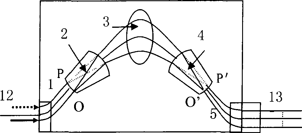
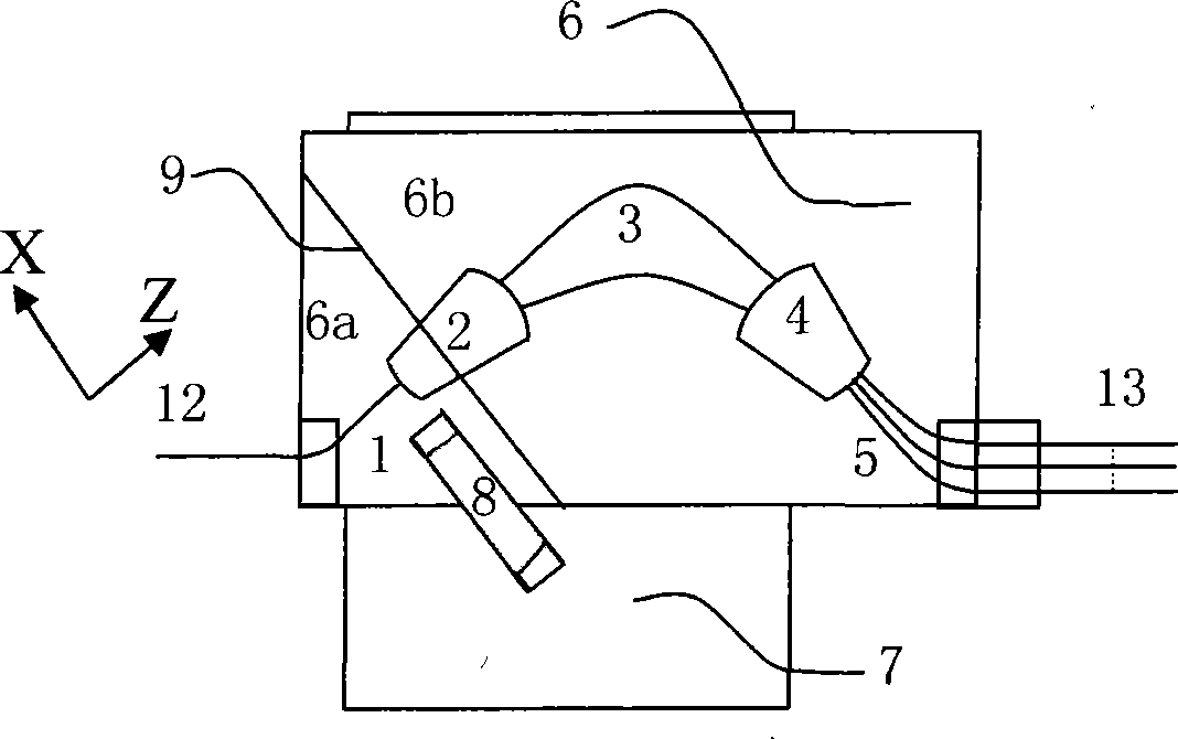
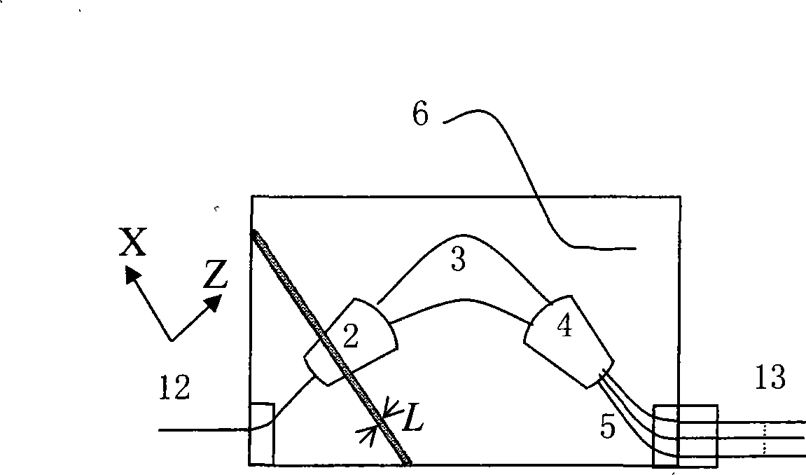
[0078] (1) if image 3 As shown, AAWG (AAWG: Athermal Arrayed waveguide grating athermal array waveguide grating); the AWG chip 6 is coupled, debugged and cured with the input fiber array 12 and the output fiber array 13, which is called the first coupling debugging and curing of AAWG, and the performance of all output channels of the output fiber array 13 is tested Parameter a1; for simplicity, according to the characteristics of the performance parameters of the AWG chip 6 itself, it is also possible to test only the performance parameter a1 of the 1, N / 2 and N...


PUM


Abstract

The invention provides an optimized producing method for a mobile athermal array waveguide grid based on planar waveguide, comprising the following steps; input waveguide, output and input waveguide, planar waveguide, output planar waveguide and array waveguide are jointly deposited on an AWG chip on a silicon substrate to produce AAWG; the AWG chip are coupled, debugged and solidified with an input fiber array and an output fiber array and the property parameter a1 is tested; the solidified AWG chip is divided into a first area and a second area of the AAWG and the waveguide length loss L caused by the division is tested; the second area is sliced and fixed with a second substrate and is arranged on a stationary fixture; the first area of the AAWG are fixed with a first substrate by a six-dimensional fine-tuning frame fixture, a compensation rod is arranged on the first area and the first substrate and is solidified; the second coupling and debugging are carried out on the stationary fixture with the second area and the second substrate by the six-dimensional fine-tuning frame fixture with the first area and the first substrate and the property parameters a2, a3 and a4 are tested; the first substrate and the second substrate are solidified.

Description

technical field [0001] The invention relates to a manufacturing method of a mobile athermal array waveguide grating based on a flat waveguide. In particular, it relates to an optimized manufacturing method based on a planar waveguide movable athermal array waveguide grating using a 6-dimensional fine-tuning frame fixture for coupling debugging. Background technique [0002] As the continuous growth of IP data services and the emergence of various broadband access services have brought about unlimited demands on bandwidth, Dense Wavelength Division Multiplexing (DWDM) technology has been flourishing. Planar light wave circuit (PLC) technology has become the mainstream industry of DWDM optical communication system because of its low cost, easy mass production, good stability, easy integration and many other characteristics. At present, the production of optical waveguides is mainly completed on substrate materials such as LiNb03, glass, InP, Si, etc. Among them, silicon-based...

Claims


Application Information

Patent Timeline
Patent Type & Authority Applications(China)
IPC IPC(8): G02B6/34
Inventor 赵秀丽马卫东丁丽祝业盛周天红
Owner GUANGXUN SCI & TECH WUHAN
Why Eureka
Try Eureka