Test construction for light doped drain doping region square resistor and manufacturing method thereof

A technology of sheet resistance and test structure, which is applied in semiconductor/solid-state device manufacturing, circuits, electrical components, etc., can solve the problems of film loss, small thickness of NLDD doped region, affecting the detection accuracy of NLDD doped region, etc., to avoid The effect of surface damage

Inactive Publication Date: 2009-06-17
SEMICON MFG INT (SHANGHAI) CORP
View PDF1 Cites 13 Cited by
  • Summary
  • Abstract
  • Description
  • Claims
  • Application Information

AI Technical Summary

Problems solved by technology

[0014] However, due to the small thickness of the NLDD doped region (that is, the shallower junction depth), it is easily affected by other processes, for example, when the layer or structure on the second region 104 is subjected to an acid solution cleaning process or a plasma etching process. etc., will cause defects (Film Lost) such as surface damage and film loss in the NLDD-doped region, which will affect the test accuracy of the sheet resistance of the NLDD-doped region, thereby affecting the detection accuracy of the NLDD-doped region; when the NLDD-doped region is detected When the sheet resistance of the region does not meet the requirements, it cannot be determined whether it is caused by the NLDD doping process or the defect of the NLDD doping region

Method used


Image

  • Test construction for light doped drain doping region square resistor and manufacturing method thereof
  • Test construction for light doped drain doping region square resistor and manufacturing method thereof
  • Test construction for light doped drain doping region square resistor and manufacturing method thereof

Examples


Embodiment Construction

[0049] The specific embodiments of the present invention will be described in detail below in conjunction with the accompanying drawings.

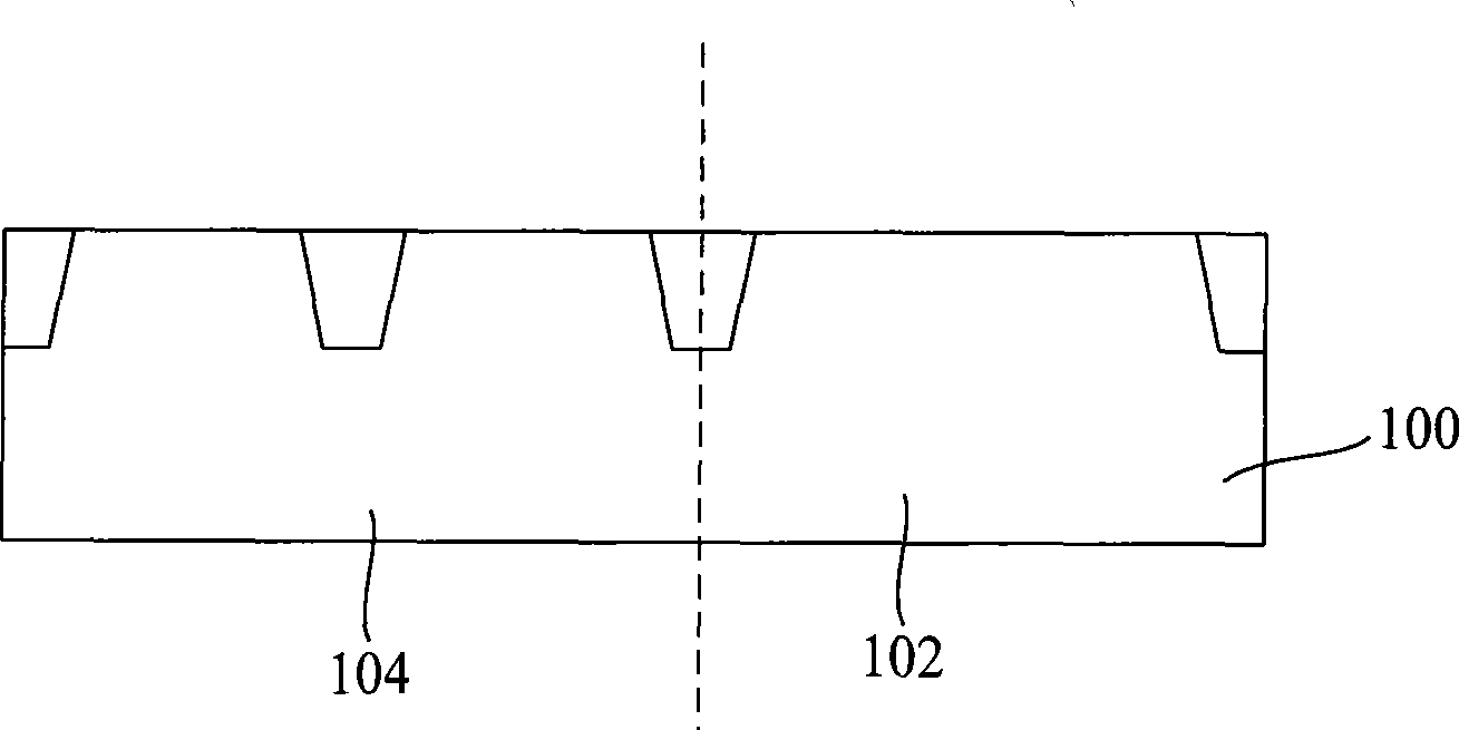
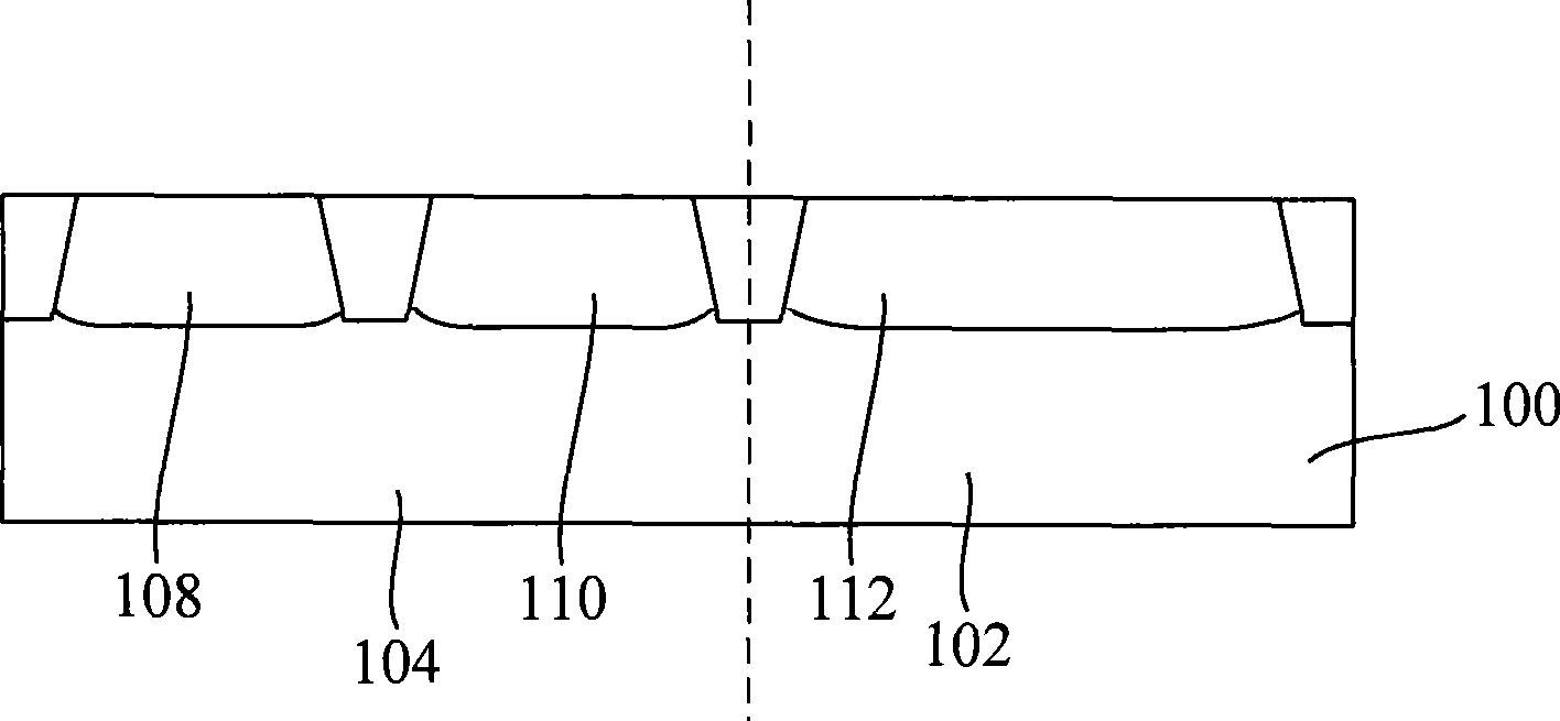
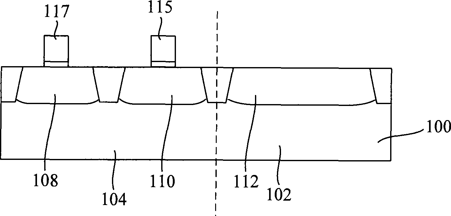
[0050] When detecting the LDD doping process, it is necessary to form the LDD doping region through the LDD doping process and measure the sheet resistance of the LDD doping region. Usually, in order to save time and cost, multiple test structures including LDD doping regions are formed on a semiconductor substrate, so as to test the entire manufacturing process of semiconductor devices including the LDD doping process. The invention provides a method for manufacturing the test structure of the sheet resistance of the LDD doped region, which can be manufactured synchronously with other test structures, and can protect the LDD doped region from being affected by other manufacturing processes, so that the LDD doped region The sheet resistance can more accurately reflect whether the LDD doping process meets the requirements.

[0051] Figur...


PUM


Abstract

A manufacturing method for a test structure of an LDD doped region square resistance comprises steps of providing a semiconductor substrate with a grid layer, wherein the semiconductor substrate is provided with a first region and a second region, patterning the grid layer, forming a grid electrode on the second region and at least two grid electrode on the first region, executing an LDD doping process to form LDD doped regions respectively in the semiconductor substrate between the grid electrodes of the first region and on the semiconductor substrate on two sides of the grid electrode of the second region, forming dielectric layers on the semiconductor substrate on the grid electrodes, on the lateral walls of the grid electrodes and between the grid electrodes, etching to remove the dielectric layers on the top of the grid electrodes and remaining a part of or the total dielectric layers on the LDD doped region of the first region. The invention further provides a test structure of an LDD doped region square resistance, which can be favorable for increasing testing precision of the LDD doped region square resistance.

Description

technical field [0001] The invention relates to the technical field of semiconductor manufacturing, in particular to a lightly doped drain doped area sheet resistance test structure and a manufacturing method thereof. Background technique [0002] With the continuous development of complementary metal-oxide-semiconductor transistor manufacturing technology, the integration level is getting higher and higher, the line width of the gate is getting smaller and smaller, and the length of the conductive channel under the gate is also continuously decreasing. [0003] In order to avoid or suppress the leakage current between the source and the drain caused by the shortening of the conductive channel length, the industry introduces a light doped drain (LDD) implantation process, that is, the source and drain are heavily doped Previously, shallow junction implants were performed with ions of higher molecular weight. [0004] In the LDD process, the implantation energy needs to be l...

Claims


Application Information

Patent Timeline
Patent Type & Authority Applications(China)
IPC IPC(8): H01L21/00H01L23/544
Inventor 叶好华毛刚何德飚
Owner SEMICON MFG INT (SHANGHAI) CORP
Why Eureka
Try Eureka