Photovoltaic devices having conductive paths formed through the active photo absorber

A solar photovoltaic and photovoltaic module technology, applied in the field of large-area photovoltaic solar modules, can solve problems such as large resistance and loss of active area of ​​solar cells

Inactive Publication Date: 2009-06-17
TERRA SOLAR GLOBAL
View PDF7 Cites 16 Cited by
  • Summary
  • Abstract
  • Description
  • Claims
  • Application Information

AI Technical Summary

Problems solved by technology

The interconnection between the front ZnO and the back Mo often presents a large resistance (inferior contact)
Furthermore, removing the film often results in excessive loss of the active area of ​​the solar cell due to the need to maintain some margin of safety

Method used


Image

  • Photovoltaic devices having conductive paths formed through the active photo absorber
  • Photovoltaic devices having conductive paths formed through the active photo absorber
  • Photovoltaic devices having conductive paths formed through the active photo absorber

Examples


Embodiment Construction

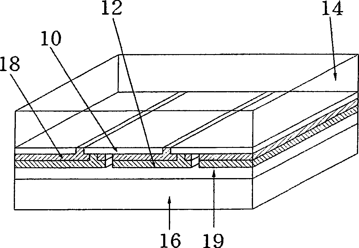
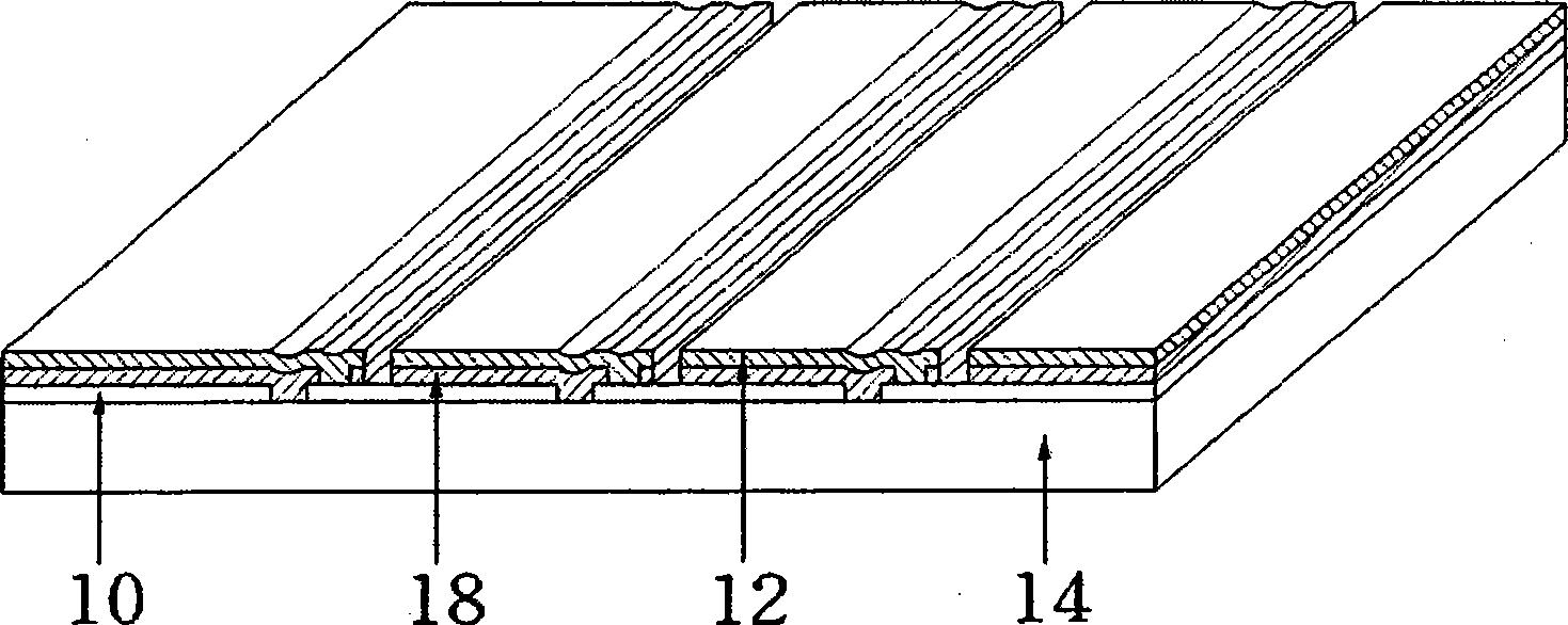
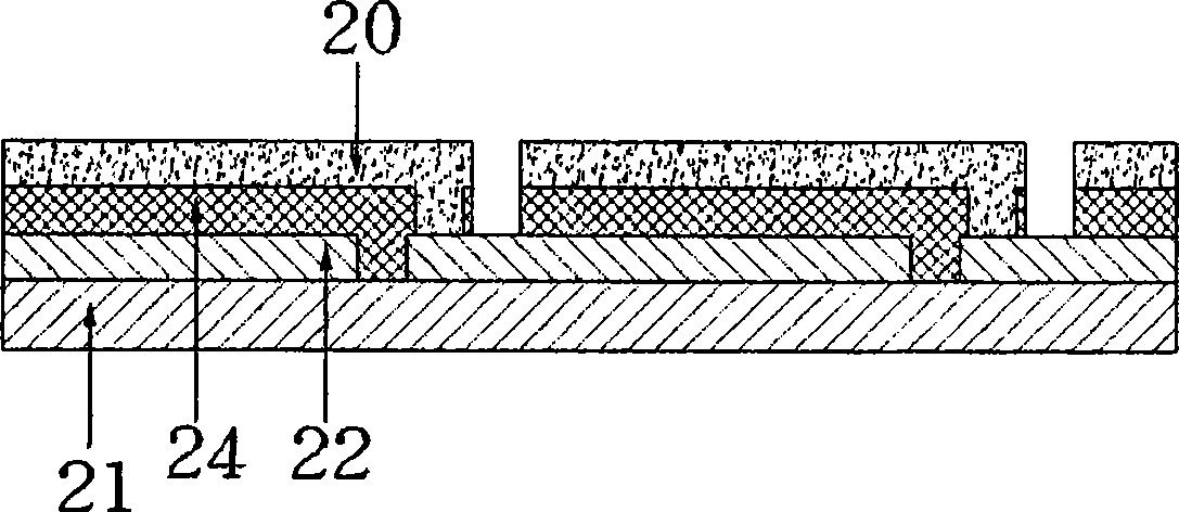
[0055] The present invention will be described in terms of CIGS PV (photovoltaic, PV) solar modules. However, it will be apparent to those skilled in the art that light-absorbing photovoltaic films other than CIGS can be used in the practice of the present invention. Furthermore, the term "TCO" as used herein shall include any suitable transparent conductive film including those comprising a buffer layer such as taught in the Shafarman & Stolt reference cited therein.

[0056] In general, according to the invention, a solar electric module comprises an array of interconnected thin-film PV solar cells in series formed on a substrate. Each cell of the array includes a back electrode spaced from the back electrode of an adjacent cell, a light-absorbing PV film in contact with the back electrode of a cell and extending at least partially to the back electrode of the adjacent cell, a TCO on the PV film A front electrode, the small portion of the PV film is located on a small porti...


PUM


Abstract

A solar PV module comprises an array of serially interconnected spaced PV solar cells on a common substrate, each cell comprising a 1st electrode on said substrate, an active PV film on the 1st electrode, a 2nd electrode, at least one of said electrodes being light transmitting and wherein the 2nd electrode of the nth solar cell of the array is connected to the 1st electrode of the succeeding, (n+1)th cell of the array via a portion of PV film which has a substantially higher conductivity than the remainder of the PV film. The novel structure of the present invention is achieved by substantially increasing the conductivity of a continuous light absorbing PV film in the area of desired electrical contact by doping the film in the desired areas.

Description

technical field [0001] The present invention relates to large area photovoltaic (PV) solar modules and methods of manufacturing the modules. Background technique [0002] The single cell voltage of most solar cells is too low to be directly applicable or efficiently used in many applications. For example, copper-indium-gallium-diselenide (CuIn x Ga 1-x Se 2 , or abbreviated as CIGS) material, the single cell voltage, depending on the composition of the CIGS material (absorber of the solar cell), lies between 0.5 and 0.8 volts (volts). [0003] Compared with the traditional PV module process based on crystalline silicon wafers, one of the advantages of thin-film photovoltaic (PV) process technology is that it can monolithically integrate individual modules when used to manufacture solar cells on the same substrate in a large area. Solar cells without relying on the cumbersome and laborious cell connections (eg, series and / or parallel) used in the industrial production of ...

Claims


Application Information

Patent Timeline
Patent Type & Authority Applications(China)
IPC IPC(8): H01L27/142H01L23/522H01L21/82H01L21/768
CPCH01L31/022466H01L31/042H01L31/1884Y02E10/50Y02E10/541H01L31/03923H01L31/0465
Inventor 李沅民
Owner TERRA SOLAR GLOBAL
Why Eureka
Try Eureka