
Ion beam apparatus and method for ion implantation

An ion implantation, ion beam technology, applied in discharge tubes, circuits, electrical components, etc., can solve problems such as limited field strength and size

Inactive Publication Date: 2009-06-24
SEMEQUIP
View PDF1 Cites 14 Cited by
  • Summary
  • Abstract
  • Description
  • Claims
  • Application Information

AI Technical Summary

Problems solved by technology

Third, relatively high-mass molecular ions tend to limit single-atom implantation energies to only a few keVs due to the limited field strength and size of conventional analyzer magnets (and other magnet components if used)

Method used


Image

  • Ion beam apparatus and method for ion implantation
  • Ion beam apparatus and method for ion implantation
  • Ion beam apparatus and method for ion implantation

Examples


Embodiment Construction

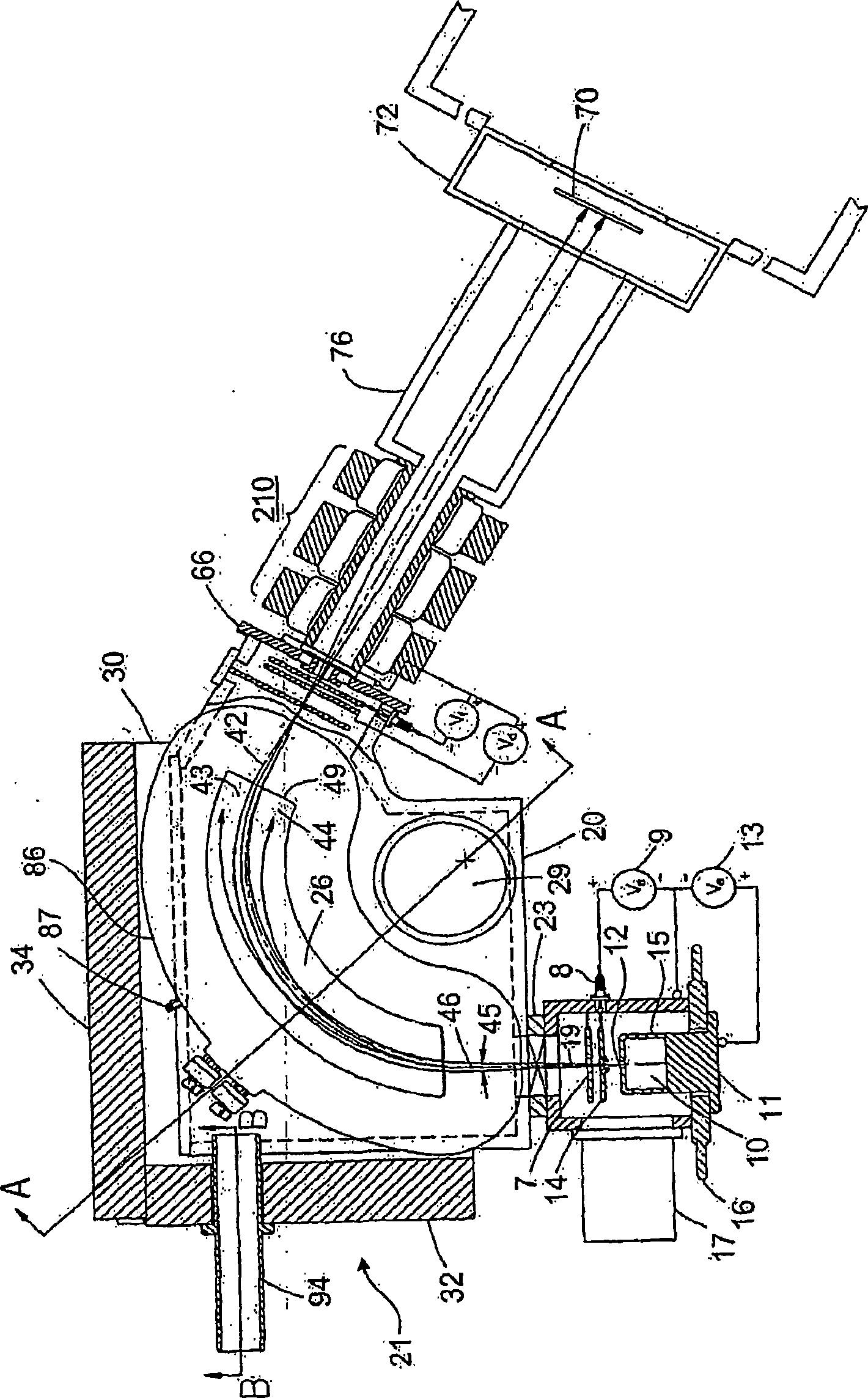
[0112] Referring now to the drawings, wherein like parts are referenced by like reference numerals and functionally similar parts are referenced by like reference numerals primed, figure 1 Schematic illustration of one embodiment of an ion implanter beamline that can be used to efficiently implant electrical dopants containing elements located on either side of Group IV elements C, Si, Ge, and Sn of the periodic table Molecular ions of multiple atoms of substances such as elements B, P, As, Sb, and In, and can also be used to efficiently implant molecular ions of multiple atoms containing elements such as C, Si, or Ge that are useful Used to modify semiconductor substrates to achieve, for example, amorphization, dopant diffusion control, stress engineering, or gettering of defects. The molecular ions can be used to fabricate integrated circuits with critical dimensions of 60 nm and smaller. Hereinafter, the ions will be collectively referred to as "cluster" ions.

[0113] Th...


PUM


Abstract

A multipurpose ion implanter beam line configuration constructed for enabling implantation of common monatomic dopant ion species and cluster ions, the beam line configuration having a mass analyzer magnet defining a pole gap of substantial width between ferromagnetic poles of the magnet and a mass selection aperture, the analyzer magnet sized to accept an ion beam from a slot-form ion source extraction aperture of at least about 80 mm height and at least about 7 mm width, and to produce dispersion at the mass selection aperture in a plane corresponding to the width of the beam, the mass selection aperture capable of being set to a mass- selection width sized to select a beam of the cluster ions of the same dopant species but incrementally differing molecular weights, the mass selection aperture also capable of being set to a substantially narrower mass-selection width and the analyzer magnet having a resolution at the mass selection aperture sufficient to enable selection of a beam of monatomic dopant ions of substantially a single atomic or molecular weight.

Description

technical field [0001] The field of the invention relates to the implantation of ions into semiconductor wafers and other substrate targets. Specifically, it relates to the efficient implantation of molecular ions containing electrical dopant species on either side of the group IV elements C, Si, Ge and Sn of the periodic table (e.g. elements B, P, As, Sb and In), and also for efficient implantation of molecular ions containing multiple atoms of elements such as C, Si, or Ge, which are now used to modify semiconductor substrates to achieve, for example, amorphization, doping Dopant diffusion control, stress engineering or gettering of defects. The molecular implants, especially those using ions with a large number of associated atoms (ie, 4 or more), are useful for fabricating integrated circuits with critical dimensions of 60 nm or less. The field of the invention also relates to implanter beamline configurations that are also suitable for commonly used monatomic dopant ion...

Claims


Application Information

Patent Timeline
Patent Type & Authority Applications(China)
IPC IPC(8): G21K5/10
CPCH01J37/05H01J2237/057H01J2237/31703H01J2237/0044H01J37/09H01J2237/14H01J2237/0492H01L21/26513H01J2237/047H01J37/3171H01J2237/30477H01J2237/0455H01L21/26566G21K5/10
Inventor 希尔顿·F·格拉维什达勒·康拉德·雅各布森托马斯·N·霍尔斯基萨米·K·哈赫托
Owner SEMEQUIP
Learn More