Method for improving non-mask photo-etching definition

A maskless lithography and resolution technology, which is applied in the field of improving the resolution of maskless lithography, can solve the problems of high feature size, inability to effectively improve resolution, and inability to meet integration requirements, and achieve high resolution. Effect

Inactive Publication Date: 2009-07-01
上海科学院 +2
View PDF1 Cites 10 Cited by
  • Summary
  • Abstract
  • Description
  • Claims
  • Application Information

AI Technical Summary

Problems solved by technology

Since the spot diameter formed by microlens focusing still reaches hundreds of nanometers, the resolution of maskless lithography cannot be effectively improved. Constrained by this, the feature size of the semiconductor device thus produced is still high, which cannot meet the ever-increasing demands. Integration requirements

Method used


Image

  • Method for improving non-mask photo-etching definition
  • Method for improving non-mask photo-etching definition
  • Method for improving non-mask photo-etching definition

Examples


Embodiment Construction

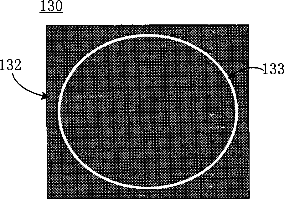
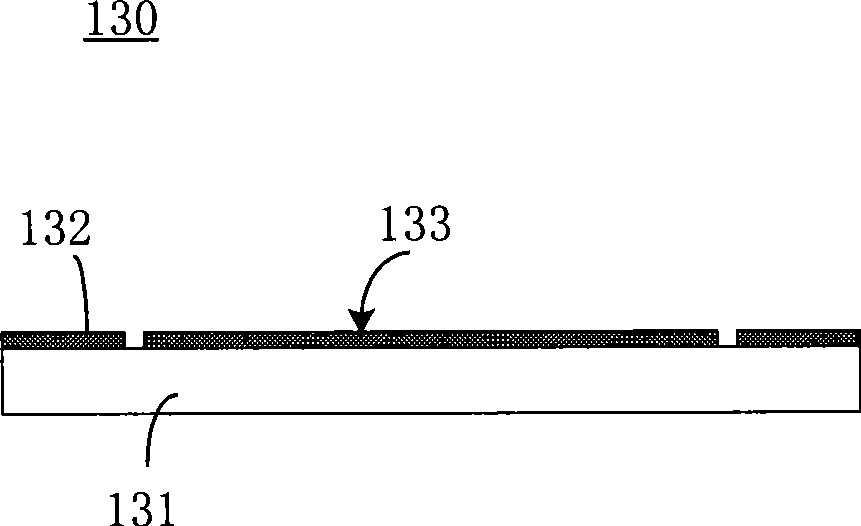
[0031] In the following description, the term "pixel point" refers to a point forming an actual required exposure pixel, and "exposure point" refers to a point formed by focusing a nanoscale light beam. It should be noted that in the context of the present invention, a "point" is an area occupying a certain two-dimensional distribution.

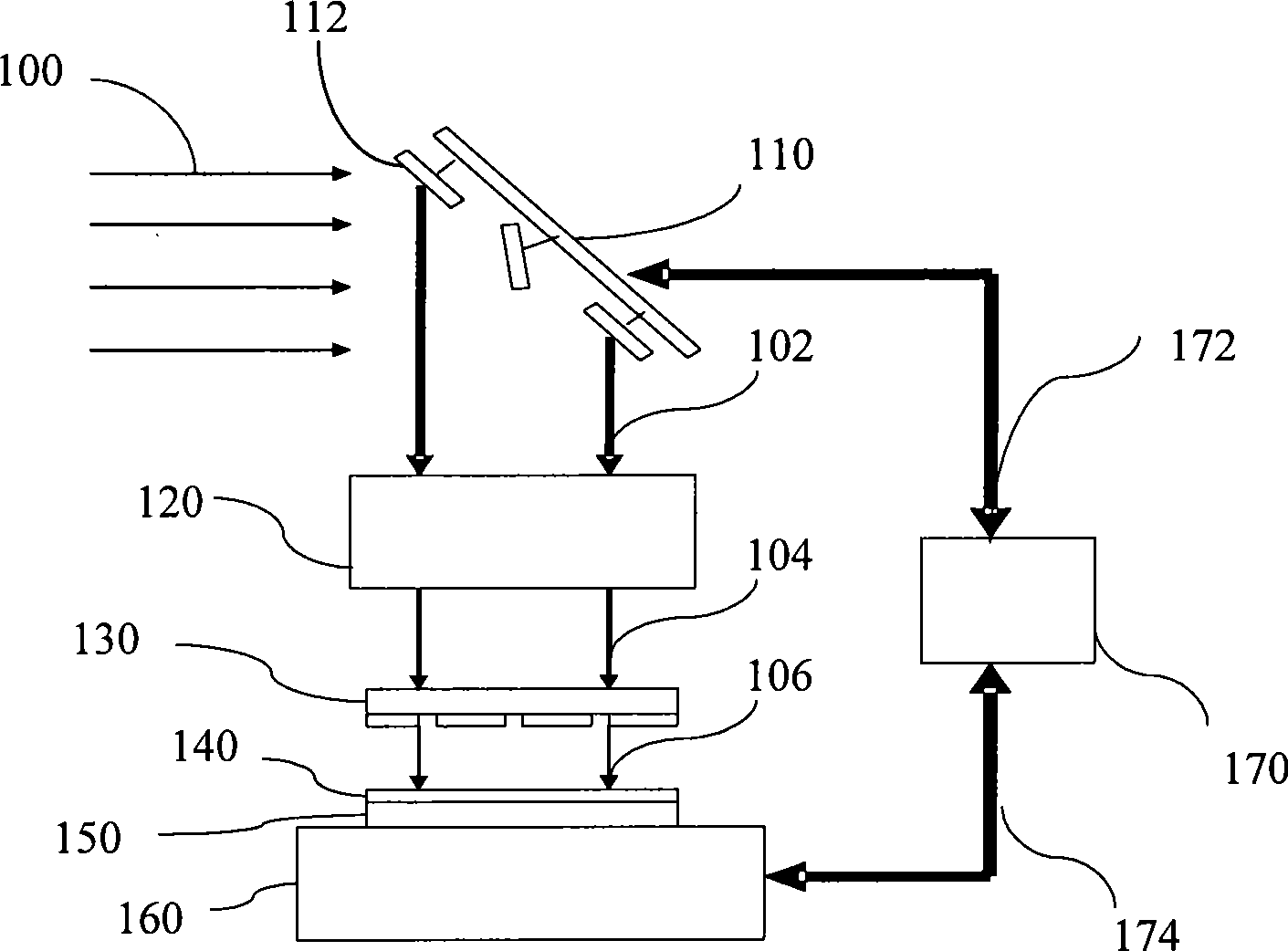
[0032] First please refer to figure 1 As shown, the structure of a maskless lithography system according to an embodiment of the present invention is as follows. A light source (not shown) that provides light 100 for exposure, such as ultraviolet light or laser light. A micro-mirror array 110 has a plurality of micro-mirrors 112 with controllable reflection directions on it, and each micro-mirror 112 can choose whether to reflect the light beam irradiated by the light source to the optical projection device 120 by changing its reflection direction, that is, The "on" and "off" controls are performed to form a micro-beam 102 with a width of a...


PUM


Abstract

The invention relates to a method for increasing maskless photo-etching resolution ratio , which is used to utilize a focusing element array to focus a patterned beam array, thereby forming a photo-etching patterns formed by a plurality of light spots in h(x, y) two-dimensional distribution on an exposed element, wherein the method enables the exposed element and the focusing element to relatively step along a first direction and a second direction to sequentially expose and form a plurality of groups of pixels, the step length moving at every time is smaller than the diameter of a light spot formed by each focusing element, thereby enabling the exposure pixel pattern of which the light intensity is larger than an exposure critical value to form the pixel in light intensity distribution formed by mutually overlapping more than one light spot on each pixel point, and then higher photo-etching resolution ratio can be obtained when the resolution ratio of the focusing element is limited.

Description

technical field [0001] The invention relates to a maskless lithography technology, in particular to a method for improving the resolution of the maskless lithography. Background technique [0002] In traditional projection optical lithography, the pattern on the mask is reduced several times (usually 4-10 times) by an optical system and projected onto the photoresist. Then, a reduced mask pattern can be obtained on the photoresist through development. [0003] With the development of semiconductor technology, the feature size of integrated circuits (Integrated Circuits, IC for short) is shrinking day by day, and traditional photolithography is facing more and more challenges, one of which is the cost and manufacturing time of masks. The price of a set of masks for 90nm integrated circuits is as high as 1 million US dollars, and the manufacturing cycle is as long as 3 months, and the proportion as high as 70% may not be used. For low-volume IC production (such as custom int...

Claims


Application Information

Patent Timeline
Patent Type & Authority Applications(China)
IPC IPC(8): G03F7/20G03F7/00
Inventor 阮巍
Owner 上海科学院
Why Eureka
Try Eureka