Check patentability & draft patents in minutes with Patsnap Eureka AI!

Bandgap refernce voltage generating circuit

A technology of reference voltage and generating circuit, applied in the direction of circuit, electrical components, adjusting electric variables, etc., can solve the problems that cannot be placed in a high state, the output voltage of the bandgap circuit is not set, and the operating time of the startup circuit is slow, etc. Achieve the effects of improving stability, stabilizing output voltage, and stabilizing startup

Inactive Publication Date: 2009-07-01
DONGBU HITEK CO LTD
View PDF0 Cites 16 Cited by
  • Summary
  • Abstract
  • Description
  • Claims
  • Application Information

AI Technical Summary

Problems solved by technology

Then, when the sleep mode is switched to the active mode, when the mismatch between the input transistors of the operational amplifier exceeds the allowable amount or when the startup circuit does not operate normally, the output voltage of the bandgap circuit may not be set and cannot be put in high state
[0009] Therefore, the related reference voltage generating circuit has a problem in that, when the sleep mode is switched to the operating mode, the operational amplifier does not have a stable operating point due to the slow operation time (slow operation time) caused by the start-up circuit.

Method used


Image

  • Bandgap refernce voltage generating circuit
  • Bandgap refernce voltage generating circuit
  • Bandgap refernce voltage generating circuit

Examples


Embodiment Construction

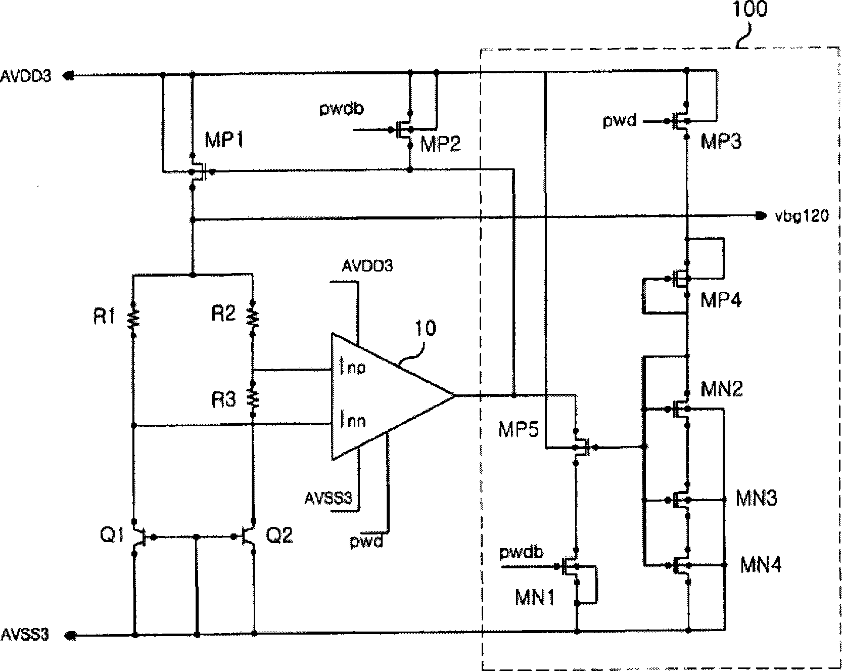
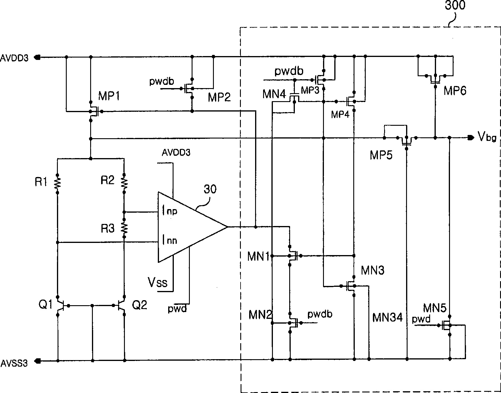
[0017] example image 3 is a circuit diagram of a bandgap reference voltage generating circuit according to an embodiment of the present invention. The bandgap reference voltage generation circuit may include: bipolar transistors Q1 and Q2, resistors R1, R2 and R3, an operational amplifier 30, PMOS transistors MP1, MP2, MP3, MP4, MP5 and MP6 and NMOS transistors MN1, MN2, MN3, MN4 and MN5.

[0018] The collectors of the bipolar transistors Q1 and Q2 may be connected to the lower limit supply voltage AVSS3 at the lowest level. The difference in emitter-base voltage between bipolar transistors Q1 and Q2 can be used to generate the reference voltage. Resistors R1 , R2 and R3 may be connected to the emitters of bipolar transistors Q1 and Q2 and to the input of operational amplifier 30 . The operational amplifier 30 outputs a constant voltage based on the reference voltage and the inverted reference voltage.

[0019] The first PMOS transistor MP1 and the second PMOS transistor ...


PUM


Abstract

A bandgap reference voltage generating circuit, includes: at least two bipolar transistors; an operational amplifier; a first PMOS transistor; and a second PMOS transistor whose source is connected to the upper limit power supply voltage and which supplies the reference current to the bipolar transistors. Further, the bandgap reference voltage generating circuit includes a third PMOS transistor whose source is connected to the upper limit power supply voltage; a fourth PMOS transistor whose source is connected to the upper limit power supply voltage and gate is connected to a drain of the third PMOS transistor; a first NMOS transistor whose source is connected to the lower limit power supply voltage and drain is connected to a drain of the fourth PMOS transistor; and a second NMOS transistor whose drain is connected to the operational amplifier and gate is connected to the drain of the first NMOS transistor.

Description

[0001] This application claims priority from Korean Patent Application No. 10-2007-0137125 (filed on December 26, 2007), the entire contents of which are hereby incorporated by reference. technical field [0002] The present invention relates to a bandgap reference voltage generating circuit (bandgap reference voltage generating circuit), and more particularly, to a bandgap reference voltage generating circuit suitable for switching from a sleep mode to an operating mode. Achieve fast start-up and obtain stable bandgap output. Background technique [0003] In a semiconductor integrated circuit, the reliability of the entire system is improved by stably maintaining an internal biasing reference voltage. That is, even if the external power supply voltage (external power supply voltage), temperature or process changes, the devices in the integrated circuit can work without being affected by changes in the external power supply voltage, temperature or process. For this purpose,...

Claims


Application Information

Patent Timeline
IPC IPC(8): G05F3/16
CPCG05F3/30G05F1/10G11C7/14H01L27/04
Inventor 赵殷相
Owner DONGBU HITEK CO LTD
Features
  • R&D
  • Intellectual Property
  • Life Sciences
  • Materials
  • Tech Scout
  • Unparalleled Data Quality
  • Higher Quality Content
  • 60% Fewer Hallucinations
Learn More