
Single electron transistor based on ordered mesoporous and preparation method thereof

A single-electron transistor and mesoporous technology, applied in semiconductor/solid-state device manufacturing, circuits, electrical components, etc., can solve the problems of disordered arrangement of quantum dots, excessive size of quantum dots, poor isolation performance of quantum dots, etc., to achieve isolation Good performance, improved reliability, and high on/off ratio

Inactive Publication Date: 2011-06-15
NAT UNIV OF DEFENSE TECH
View PDF8 Cites 0 Cited by
  • Summary
  • Abstract
  • Description
  • Claims
  • Application Information

AI Technical Summary

Problems solved by technology

[0008] The technical problem to be solved by the present invention is to use ordered mesopores with regular arrangement as the quantum dots in the preparation of single electron transistors to solve the problems of excessive size of quantum dots, disordered arrangement of quantum dots and poor isolation performance of quantum dots in current single electron transistors. Dot templates to prepare single-electron transistors based on ordered mesoporous holes, so that this single-electron transistor can work normally at room temperature, and is convenient for large-scale preparation and integration

Method used


Image

  • Single electron transistor based on ordered mesoporous and preparation method thereof
  • Single electron transistor based on ordered mesoporous and preparation method thereof
  • Single electron transistor based on ordered mesoporous and preparation method thereof

Examples


Embodiment Construction

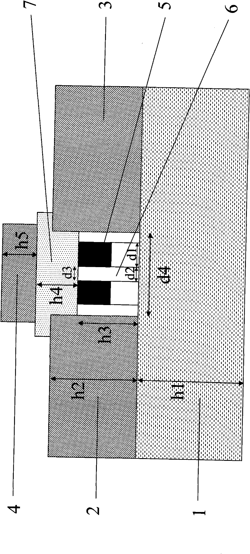
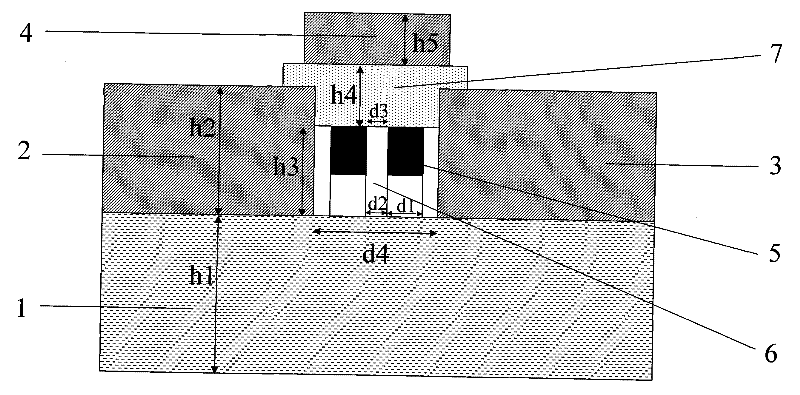
[0033] figure 1 It is a side view of the single-electron transistor based on the ordered mesopore of the present invention. The bottom is the substrate 1, using clean and flat glass, single crystal silicon or aluminum oxide deposited on the surface or oxidized to silicon dioxide, and its thickness h1 is 400um~2mm; the source 2 and drain 3 are prepared on the substrate 1 Surface, the thickness h2 is 5nm-500nm; the ordered mesoporous layer 6 is prepared on the surface of the substrate 1, the thickness h3 is 50nm-500nm, the pore diameter d1 of the ordered mesoporous is 1nm-8nm, and the pores of the ordered mesoporous The wall thickness d2 is 1 nm to 3 nm; the ordered mesoporous layer 6 is assembled with nanoparticles 5, and the size d3 of the nanoparticles 5 is 0.5 nm to 8 nm; the distance between the source 2 and the drain 3 is d4 5nm to 20nm; the insulating layer 7 is on the source 2, the drain 3 and the ordered mesoporous layer 6, and its thickness h4 is 3nm to 30nm; the gate...


PUM


Abstract

The invention discloses a single-electron transistor based on ordered mesopores and the fabrication method thereof, which can solve the problems of the prior single-electron transistors, such as large quantum dot size, disordered arrangement of the quantum dots and poor isolation performance of the quantum dots. The single-electron transistor based on ordered mesopores consists of a substrate, a source, a drain, a gate and an ordered mesopore layer and an insulation layer, wherein nanoparticles serving as the quantum dots of the single-electron transistor are assembled in the ordered mesopores of the ordered mesopore layer. The fabrication method comprises the following steps: preparing the substrate; then fabricating the ordered mesopore layer, the source and the drain; fabricating the insulation layer next; and finally fabricating the gate. With the adoption of the method, quantum dots with the size of 0.5 to 0.8 nm and ordered arrangement, so that the single-electron transistor canoperate at normal temperature with the advantages of high reliability and convenient fabrication and integration.

Description

technical field [0001] The invention relates to a single-electron transistor and a preparation method thereof, in particular to a single-electron transistor based on ordered mesopores and a method for preparing the device by using nanometer chemical and physical processing methods. Background technique [0002] Integrated circuits with metal-oxide-semiconductor field-effect transistor (MOSFET) devices as the mainstream have been developing rapidly following Moore's law. The minimum feature size of the current MOSFET has reached 65nm. As the feature size enters the nanometer level, MOSFETs exhibit strong quantum effects, and logic functions are severely challenged. Therefore, it is imminent to develop electronic logic devices that can work normally at the nanoscale, and has become a research hotspot in the field of integrated circuit manufacturing. [0003] Single-electron transistors have the advantages of small size, fast speed, low power consumption, and large-scale inte...

Claims


Application Information

Patent Timeline
Patent Type & Authority Patents(China)
IPC IPC(8): H01L29/78H01L21/336B82B3/00
Inventor 池雅庆张学骜仲海钦方粮常胜利贾红辉隋兵才周海亮孙鹤张超杨学军王正明唐玉华
Owner NAT UNIV OF DEFENSE TECH
Learn More