Production method for self-aligned metallic oxide thin-film transistor

A technology of oxide film and manufacturing method, which is applied in semiconductor/solid-state device manufacturing, semiconductor devices, electrical components, etc., can solve the problems of discrete characteristics, non-self-alignment of device structure, large parasitic components of devices, etc., and achieve increased complexity , to avoid parasitic effects, the effect of increased power consumption

Active Publication Date: 2009-07-22
BOE TECH GRP CO LTD
View PDF0 Cites 41 Cited by
  • Summary
  • Abstract
  • Description
  • Claims
  • Application Information

AI Technical Summary

Problems solved by technology

However, one of the main problems with the fabrication methods of zinc oxide thin film transistors invented so far is that the formed d

Method used


Image

  • Production method for self-aligned metallic oxide thin-film transistor
  • Production method for self-aligned metallic oxide thin-film transistor
  • Production method for self-aligned metallic oxide thin-film transistor

Examples


Embodiment Construction

[0030] The present invention will be further described in detail below in conjunction with the accompanying drawings through the embodiments.

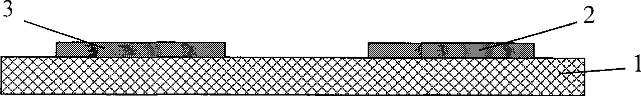
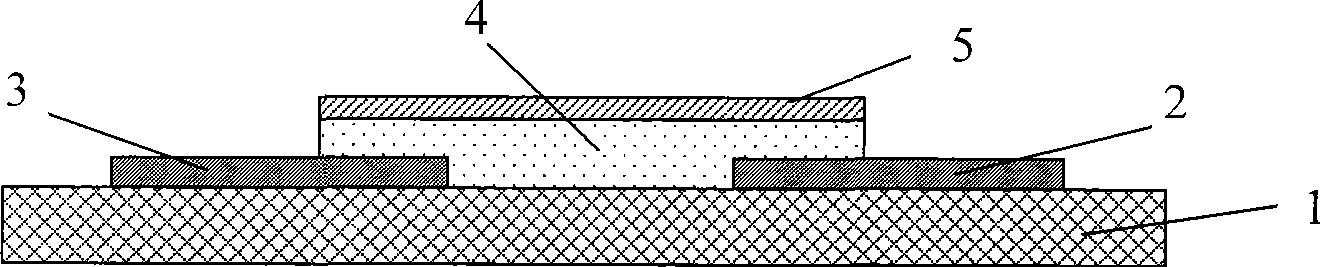
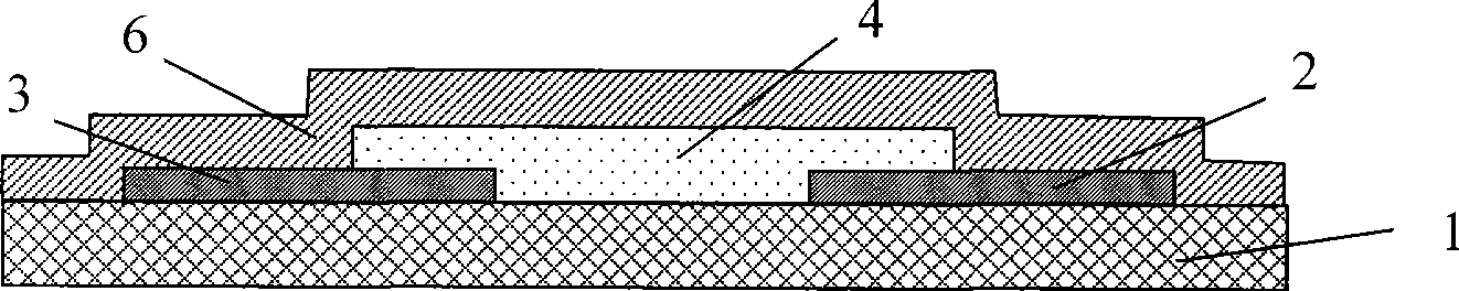
[0031] The sectional view of the thin film transistor that the present invention makes is as Figure 6 shown. The transistor is formed on a glass substrate 1 and includes a gate electrode 8, a channel region 4, a gate dielectric layer 6, a source region 2 and a drain region 3; the source region 2 and the drain region 3 are located on the glass substrate 1 above; the channel region 4 is a semiconductor layer located in the middle of the glass substrate 1 between the source region 2 and the drain region 3, and the two ends of the semiconductor layer are partially stacked on the source region 2 and the drain region 3 above; the gate dielectric layer 6 is located above the channel region 4 and the source region 2 and the drain region 3; the gate electrode 8 is located above the gate dielectric layer 6, and the gate electrode 8 is symmetri...


PUM


Abstract

The invention provides a method for manufacturing a self-aligned metal-oxide film transistor. First, a metal source drain region, a metal-oxide semiconductor channel region and a transparent gate medium layer are sequentially arranged on a glass substrate, then positive photoresist is coated on the gate medium layer, after pre-baking is carried out, exposure, developing and hardbaking are carried out from the back of the glass substrate, afterwards, a layer of conductive film develops with glue, then a gate electrode is obtained after stripping the photoresist and the conductive film, photoetching and etching. The method of the invention can ensure self alignment between the gate electrode and the source drain region of a component, namely, the gate electrode is symmetrically arranged right above between the source and the drain, while, length of the gate electrode is determined by the distance between the source and the drain instead of size of a mask, thus effectively avoiding ghost effect.

Description

technical field [0001] The invention relates to a method for preparing a thin film transistor, in particular to a method for preparing a self-aligned metal oxide semiconductor thin film transistor. Background technique [0002] Flat panel display technologies and devices have developed into mainstream technologies and devices for information display. For flat-panel displays, whether it is the currently dominant liquid crystal display (LCD), the light-emitting diode (OLED) display that is expected to become the mainstream of the next generation, or the flexible substrate display in the future, it is necessary to achieve large-size and high-resolution display , it is necessary to use thin film transistors as switch control elements or integrated elements of peripheral drive circuits. Currently widely used thin film transistors mainly include amorphous silicon thin film transistors and polysilicon thin film transistors. [0003] Amorphous silicon thin film transistors have th...

Claims


Application Information

Patent Timeline
IPC IPC(8): H01L21/336H01L21/027H01L29/06
Inventor 张盛东李绍娟王漪孙雷关旭东韩汝琦
Owner BOE TECH GRP CO LTD
Why Eureka
Try Eureka